Review
. 2020 Nov 6;10(11):2215.
doi: 10.3390/nano10112215.

Silicon Nanowires for Gas Sensing: A Review

Affiliations
Review

Silicon Nanowires for Gas Sensing: A Review

Mehdi Akbari-Saatlu et al. Nanomaterials (Basel). .

Abstract

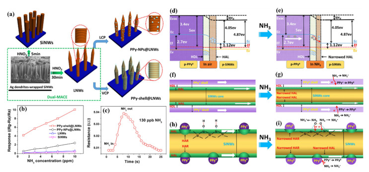
The unique electronic properties of semiconductor nanowires, in particular silicon nanowires (SiNWs), are attractive for the label-free, real-time, and sensitive detection of various gases. Therefore, over the past two decades, extensive efforts have been made to study the gas sensing function of NWs. This review article presents the recent developments related to the applications of SiNWs for gas sensing. The content begins with the two basic synthesis approaches (top-down and bottom-up) whereby the advantages and disadvantages of each approach have been discussed. Afterwards, the basic sensing mechanism of SiNWs for both resistor and field effect transistor designs have been briefly described whereby the sensitivity and selectivity to gases after different functionalization methods have been further presented. In the final words, the challenges and future opportunities of SiNWs for gas sensing have been discussed.

Keywords: bottom-up fabrication; functionalization; gas sensor; heterostructures; metal oxides; silicon nanowire; top-down fabrication.


Conflict of interest statement

The authors declare no conflict of interest.

Figures

Figure 1
Figure 1
(a) Schematic representation of a cross-section of a 10 nm SiNW produced from SOI using a 193 nm immersion lithography process incorporating resist trimming steps and over-etching. Where HM stands for hardmask, ACL for Amorphous Carbon Layer, DRAC for Dielectric Anti-Reflective Coating, and SiOC for Silicon OxyCarbide. (b) CDSEM images show LER trend with increasing dose and resist quencher concentration. Figure 1b is reproduced from [68], with permission from SPIE and the author (Alex Robinson), 2017.
Figure 2
Figure 2
Process flow of Side-wall Transfer Lithography (STL). (a) SOI substrate (b) Oxide deposition (PEOX) on SOI, (c) amorphous-Si (α-Si) on PEOX, (d) SiN hardmask, (e) lithography & etch of hardmask and dummy gate, (f) stripe photoresist and SiN, (g) SiN deposit on etched α-Si, (h) etch spacer, (i) etch Si-NW, (j) remove α-Si and PEOX then Si-NWs are formed. Fabrication of Si NWs sensor: (k) top view of Si NW arrays by optical microscope, the length of NWs is about 50 µm. (l) SEM image of Si NW arrays, the NWs width is about 30 nm, (m) cross sectional TEM image of Si NW sensors, conformal and uniform HfO2 layer are observed, which is attributed to a good isolation between electrode and the solution of cells. Figure 2k–m are reproduced from [72], with permission from IEEE, 2020.
Figure 3
Figure 3
Schematic of CVD-VLS growth of SiNWs. (a) A liquid alloy droplet Au-Si is first formed above the eutectic temperature (363 °C) of Au and Si. The continuous feeding of Si in the vapor phase into the droplet causes supersaturation of the liquid alloy, resulting in nucleation and growth of SiNWs. (b) Binary phase diagram for Au and Si showing the thermodynamics of CVD-VLS growth. Reproduced from [101], with permission from IOP Publishing, 2020. (c) SEM images of SiNWs grown on a ⟨111⟩ Si substrate at 525 °C for 120 min by MBE. (d) TEM cross section image of a SiNW with Au on top. (e) Schematic representation of the MBE NW growth. I1 and I2 are fluxes of Si adatoms directed to the gold cap. Reproduced from [102], with permission from American Vacuum Society, 2020.
Figure 4
Figure 4
(a) Schematic diagram of the SiNW growth system. The output from a pulsed laser (1) is focused (2) onto a target (3) located within a quartz tube; the reaction temperature is controlled by a tube furnace (4). A cold finger (5) is utilized to collect the droplets because of the introduced carrier gas (6, left) through a flow controller and exits (6, right) into a pumping system. (b) Proposed PLD growth model. (c) TEM image of the SiNWs obtained from the cold finger. Scale bar, 100 nm. (d) TEM image of a SiNW; scale bar is 10 nm. (e) High resolution TEM image of the crystalline SiNW and amorphous SiOx sheath. (f) Schematic diagram of the thermal evaporation system, where the SiO powder is located at A, and the grown SiNWs are located at B. (g) The schematic diagram of oxide-assisted growth mechanism. (h) TEM image showing the morphologies of randomly oriented SiNWs. Reproduced from [102], with permission from American Vacuum Society, 2020.
Figure 5
Figure 5
Schematic of (a)i a separate horizontal SiNW and (a)ii and (a)iii show conduction path in n-type (which is through inner part of SiNW) and p-type (which is through outer shell of SiNW) respectively. (b)i multiple vertical SiNWs with NW/NW junction barriers shown in (b)ii for n-type and (b)iii for p-type.
Figure 6
Figure 6
Schematic of SiNW-FET as gas sensors when NWs are formed (a) horizontally and (b) vertically.
Figure 7
Figure 7
(a) Schematic illustration of the fabrication process for a rough SiNW array. (b) Sensor response as a function of NO2 concentration at room temperature for normal smooth SiNWs and rough SiNWs. (c) Dynamic response curve of the rough SiNWs array sensor to varying concentrations of NO2. Reproduced from [133], with permission from Springer Nature, 2020.
Figure 8
Figure 8
Schematic illustration of the etching models for the formation of (a) separating and (b) bundling SiNWs using MACE process. The SEM micrographs show in the part (a) uniform Ag nanoparticles formed on the untreated hydrophilic substrate and in the part (b) irregular Ag nanoflakes formed on the HF pretreated-induced hydrophobic substrate. Reproduced from [111], with permission from publisher John Wiley and Sons, 2020.
Figure 9
Figure 9
Schematic view of grounded (a) and suspended (b) sidewall spacer polycrystalline SiNWs. (c) SEM image of suspended polycrystalline SiNWs based sensing structure. (d) Relative response (Sg = (Rg − R)/Rg) of the sensors vs. the ammonia concentration for both suspended and grounded SiNWs resistors. Reproduced from [135].
Figure 10
Figure 10
(a) Schematic view and (b) SEM image of the inter-digitated comb-shaped SiNWs based sensor. (c) Relative sensitivity to ammonia detection versus the phosphine to silane ratio (the insert shows the effect of the doping level on the sensitivity to ammonia detection molecules). Reproduced from [136], with permission from John Wiley and Sons, 2020.
Figure 11
Figure 11
Schematic illustration of H2 sensing mechanisms in (a) n- and (c) p-type Pd-coated SiNW arrays based on carrier concentration. Resistance variation with time for 0.2% H2 depending on the major carrier types in (b) n- and (d) p-type Pd-coated Si NW arrays. Reproduced from [139], with permission from Elsevier, 2020.
Figure 12
Figure 12
Schematic illustration of the change in contact resistance at the metal (Pd)-semiconductor (Si) junction: (a) formation of Schottky barrier in an n-type SiNW before the exposure of H2, (b) formation of Ohmic contact in the n-type SiNW after the exposure of H2, (c) formation of Ohmic contact in the p-type SiNW before the exposure of H2, and (d) formation of Schottky barrier in the p-type SiNW after the exposure of H2. Reproduced from [139], with permission from Elsevier, 2020.
Figure 13
Figure 13
Working principle of H2 sensing of Pd-SiNWs: (a) at room temperature, (a-i) depletion of charge carrier (electron) in SiNW (n-type) by negatively charged adsorbed oxygens (red dots) and (a-ii) accumulation of charge carrier by desorbing oxygen with H2O formation under H2 gas exposure; (b) Faster and higher response with self-heating of Pd-SiNW because of (b-i) more depletion of charge carrier due to more adsorbed oxygen and (b-ii) fast reaction rate with H2; Low interfering gas effect (H2O and CO) with self-heating; (c) Lowered power consumption by reducing heat loss through the substrate by changing from substrate-bound SiNW to suspended SiNW. Reproduced from [141], with permission from American Chemical Society, 2019.
Figure 14
Figure 14
SEM images of a (a) substrate bound, and (b) suspended SiNW. A comparison between the substrate-bound and suspended Pd-SiNW sensors is shown in (c) showing responses with various self-heating powers (red arrows: direction of self-heating power increment (from 41 to 147 μW for the suspended Pd-SiNW and from 205 to 1172 μW for the substrate-bound Pd-SiNW)). Reproduced from [141], with permission from American Chemical Society, 2019.
Figure 15
Figure 15
Schematic illustration of gas sensing mechanism of (a,b) bare p-SiNW and (ce) Ag modified rough p-SiNW sensor, (f) the corresponding description of symbols, (g) dynamic response curves of the sensors based on Ag NPs@RNWs to varying concentration of NO2 at room temperature and (h) response of the Ag NPs@RNWs sensor to different gases: the concentration of NO2 at 0.3 ppm and others at 10 ppm. Reproduced from [150] and [151], with permission from American Chemical Society, 2017 and Elsevier, 2020.
Figure 16
Figure 16
Schematics and energy band diagrams of different contact structures before and after being exposed to NO2 for (a) p-type SiNWs contact structure, (b) n-type SiNWs contact structure, p-n homojunction under forward voltage (c) and reverse voltage (d). Reproduced from [137], with permission from RSC Pub, 2020. (●, electron; ○, hole).
Figure 17
Figure 17
SiNWs/TiO2 core-shell structures for CH4 sensing: (i) SEM images of SiNWs before (a,b) and after (d,e) TiO2 deposition and TEM images of SiNW (c) and SiNW/TiO2 (f) structures; (ii) (a) n- and p-type SiNWs based sensors (bare, thermal oxidized and TiO2 coated) responses to 100 ppm of CH 4 at RT, (b) the conductive response of n-SiNWs/TiO2 sensor to 100 ppm of CH4 at different temperatures.; (iii) schemes of RT CH4 sensing mechanism for (a) p-SiNWs/TiO2, (b) n-SiNWs/TiO2 Reproduced from [156], with permission from American Chemical Society, 2017.
Figure 18
Figure 18
(a) SEM images of ZnONWs/PSiNWs hybrid strictures and schemes of these structures with different ZnO coverage; (b) scheme of proposed sensing mechanism-energetic bands of ZnONWs/PSiNWs (i) before and (ii) after exposure to oxidizing gas; (c) response of the of bare PSiNWs and ZnO to NO2 at RT; (d) responses of ZnONWs/PSiNWs hybrids presented in SEM images. Reproduced from [157], with permission from Royal Society of Chemistry, 2020.
Figure 19
Figure 19
SEM and TEM images of SiNWs before (a,b) and after (c,d) ZnO deposition; (e) response of SiNWs/ZnO heterojunction to NO at RT in N2 atmosphere for both n and p-type SiNWs. Reproduced from [158], with permission from IOP Publishing, 2020.
Figure 20
Figure 20
(a,b) The side view SEM images of SiNWs/WO3 nanowires. (c) Schematic illustration for gas-sensing mechanism of SiNWs/WO3 sensor, structural model, and heterostructure models and energy band diagrams in air and in NO2. Dynamic responses of the composite (d) and the pure SiNWs (e) to 0.5–5 ppm NO2 at RT. Reproduced from [159], with permission from Elsevier, 2020.
Figure 21
Figure 21
(a) SEM images of the (i) fabricated SnO2 CGFET, (ii) close-up view of the honeycomb channel region before and (iii) after the SnO2 deposition process, (b) schematic illustration of various gas sensor structures: (i) two terminal chemiresistor, (ii) back-gated FET, (iii) platinum gate FET typically used as hydrogen sensors, and (iv) metal-oxide floating gate CGFET. (c) Conceptual illustration of the response of (i) chemiresistor and (ii) CGFET for oxidizing and reducing gases. The monotonic function of the chemiresistor results in a response to both oxidizing and reducing gases. The nonlinearity of the normally off CGFET selectively responds to the corresponding type of gas. The response of the CGFET and the control chemiresistor with different concentration for (d) ammonia and (e) O2. Reproduced from [161], with permission from American Chemical Society, 2020.
Figure 22
Figure 22
(a) SEM top and cross-section images of the SiNWs (The inset’s scale-bar is 2 μm). (b) the schematic diagram of process flow for a MoS2/SiNW heterojunction device, (c) I-V curves of MoS2/SiNW heterojunction in dry air, (d) I-V curves of MoS2/SiNW heterojunction at reverse voltage under varied RH values, (e) the dependence relation between sensitivity and relative humidity. (f) current response of MoS2/SiNW heterojunction to dynamic switches between dry air and varied RH valu,s at Vbias = −5 V, and (g) single-cycle response with different RH values. Reproduced from [162], with permission from Elsevier, 2020.
Figure 23
Figure 23
(a) I–V curves of MoS2/SiNW heterojunctions in air and NO2, (b) Equivalent electrical resistance model of MoS2/SiNW heterojunctions schematic illustration of using CVD to grow MoS2 nanosheets on PSiNWs, and (c) Schematic illustration of the energy band of MoS2/SiNW heterojunction structures, and (d) Dynamic response in different NO2 concentrations, and (e) response values of NO2 concentrations. Reproduced from [164].
Figure 24
Figure 24
(a) Schematic illustration of the major processes involved in the fabrication of PPy-NPs@LNWs and PPy-shell@LNWs, (b) Response comparison of PPy-shell@LNWs, PPy-NPs@LNWs, bare LNWs and bare SiNWs, (c) Dynamic response of PPy-shell@LNWs to 130 ppb NH3 at RT. Schematic illustrations showing the NH3-sensing mechanism of PPy-shell@LNWs and PPy-NPs@LNWs: (d,e) Energy band diagrams of a PPy-SiNWs junction in air and in NH3; (fi) conduction channel change before and after NH3 adsorption for PPy-shell@LNWs (f,g) and for PPy-NPs@LNWs (h,i). Reproduced from [166], with permission from Elsevier, 2020.
Figure 25
Figure 25
Dynamic response of the sensors based on NWs: (a) LNWs, (b) LNWs/PPy-10, (c) LNWs/PPy-20 (d), and LNWs/PPy-30, and (e) to varying concentration of NO2 at room temperature. Reproduced from [117], with permission from John Wiley and Sons, 2020.
Figure 26
Figure 26
(a) Schematic diagram of the GQDs/SiNW array-based gas sensor. (b) Sensitivity responses of the SiNWs array with and without decoration of GQDs to NO2 (500 ppm) at room temperature. (c) Energy band diagram of the GQDs/SiNW heterojunction. Reproduced from [167], with permission from IOP Publishing, 2020.
Figure 27
Figure 27
Cross-sectional SEM images of (a) n-SiNWs. (b) p-SiNWs. (c) SEM image of RGO@n-SiNWs with HF treatment, (d) Zoomed-in SEM image of RGO@n-SiNWs with HF treatment, (e) dynamic response of n-SiNWs and RGO@n-SiNWs from 0.1 to 10 ppm HCHO, (f) The response of n-SiNWs and RGO@n-SiNWs for seven types of common VOCs (10 ppm) at 300 °C. Reproduced from [115].
Figure 28
Figure 28
Plan-view image of the graphene/Si-NW heterostructure where, (a) dark graphene sheet on tips of SiNWs, (b) tilted-view image of graphene/Si NWs confirming the uniform contact between graphene and Si NWs, and (c) plan-view image of an Au film on graphene and tips of Si NWs. A continuous Au film is formed only on graphene where (d) tilted-view image of Au/graphene/Si NWs with a continuous Au film is well placed on the graphene/Si NWs, (e) fabrication process of the device. Normalized resistance responses of graphene/SiNW heterostructure molecular sensor under repeated exposures of (f) O2 and (g) H2 gases in air at room temperature. Exposure intervals of O2 and H2 gases are 10 s and 30 s, respectively. Reproduced from [168].
Figure 29
Figure 29
(a) Schematic illustration of construction of OTS-modified porous SiNWs for NO2 detection under high humidity condition, (b) Dynamic responses to 250 ppb NO2 at 65% RH for SiNWs sensor and (c) OTS/SiNWs sensor, (d) dynamic responses of OTS/SiNWs and SiNWs sensors to 50 ppb NO2 at 75% RH. (e) response value versus relative humidity and corresponding cubic fits (red line) for SiNWs sensor, (f) OTS/SiNWs sensor towards 50 ppb NO2, and (g) dynamic response of OTS/SiNWs sensor to varying concentration of NO2 at 75% RH. Reproduced from [116], with permission from Elsevier, 2020.
Figure 30
Figure 30
Sensing mechanism in the Au-functionalized SiNWs/ZnO core-shell gas sensor, (a) Formation of the depletion layers in the pristine SiNWs/ZnO core-shell layer and (b) Expansion of the electron depletion layer in the presence of Au. Reproduced from [174], with permission from Elsevier, 2020.
Figure 31
Figure 31
(a) Schematic outline showing spillover effects due to the presence of Au NPs, (b) energy band structure of ZnO/Au upon the formation of heterointerfaces, and (c) energy band structure of ZnO/p-Si prior to contact, (d) Gas response for different concentrations of H2S gas at 300 °C. Reproduced from [174], with permission from Elsevier, 2020.
Figure 32
Figure 32
(a) Fabrication processes of the Pt-functionalized TeO2-branched Si nanowires, (b) schematic diagram showing the four mechanisms being operated in the Pd-functionalized branched nanowires: (R1) modulation in the hole accumulation along the branch TeO2 nanowires, (R2) modulation of the potential barrier at the networked homojunctions between the branch TeO2 nanowires, (R3) modulation of the potential barrier at the boundaries of the nanograins and (R4) modulation of the potential barrier at the Pd-TeO2 heterojunctions (including additional Pd effects), and (c) column bar graph showing the variation of sensor responses by addition of TeO2 branches, Pd-functionalization, and varying the gas species at 50 ppm. The sensing temperature was 200 °C. Reproduced from [175], with permission from Elsevier, 2020.
Figure 33
Figure 33
Dynamic resistance curves of (a) pristine and (b) Pt-functionalized branched nanowires at NO2 concentrations of 10, 20, and 50 ppm. (c) Schematic diagram showing the four resistance mechanisms operating in Pd-functionalized branched nanowires: (R1) modulation of depletion width along the branched TeO2 nanowires (including additional Pt effects), (R2) modulation of the potential barrier at networked homojunctions between branched TeO2 nanowires, (R3) modulation of the potential barrier at boundaries of the nanograins, and (R4) modulation of the potential barrier at Si-TeO2 heterojunctions. Reproduced from [176], with permission from Elsevier, 2020.
Figure 34
Figure 34
Schematic illustrations showing the NH3-sensing mechanism of Ag-PPy@SiNWs: (a) electrical conducting paths, (b) energy band diagram of an Ag-PPy@SiNWs junction in air. Conduction channel changes (c) before and (d) after NH3 adsorption for Ag-PPy@SiNWs. (e) Schematic diagram of anti-humidity effect induced by Ag NPs. (f) Response comparison of Ag-PPy@SiNWs, PPy@SiNWs and SiNWs at room temperature. Reproduced from [177], with permission from Elsevier, 2020.
Figure 35
Figure 35
Schematic representation of (a) 3-aminopropyltrimethoxysilane grafting to the silanol-terminated surface of a SiNW, (b) the covalent modification process of the SiNW surface with melamine-terephthaldehyde-based POFs, (c) the metalation of a POF-SiNW via an in situ chemical reduction. Molecules 1–3: APTES, melamine, terephthaldehyde, respectively. SEM images of (d) bare SiNW, and (e) SiNW decorated with POFs, (f) normalized response upon exposure to 3000 ppm of methanol vapor for bare SiNW, POF-SiNW and PtNP@POF-SiNW sensors, and both (g) and (h) show the resistance of the ZnONPs-SiNW/rGO and TiO2NPs-SiNW/rGO as a function of humidity. Reproduced from [15]; and Reproduced from [178], with permission from RSC Pub, 2020.

References

    1. Tyagi D., Wang H., Huang W., Hu L., Tang Y., Guo Z., Ouyang Z., Zhang H. Recent advances in two-dimensional-material-based sensing technology toward health and environmental monitoring applications. Nanoscale. 2020;12:3535–3559. doi: 10.1039/C9NR10178K. - DOI - PubMed
    1. Nunes D., Pimentel A., Gonçalves A., Pereira S., Branquinho R., Barquinha P., Fortunato E.M.R. Metal oxide nanostructures for sensor applications IOPscience. Semicond. Sci. Technol. 2019;34:043001. doi: 10.1088/1361-6641/ab011e. - DOI
    1. Jian Y., Hu W., Zhao Z., Cheng P., Haick H., Yao M., Wu W. Gas Sensors Based on Chemi-Resistive Hybrid Functional Nanomaterials Chemi-resistive Hybrids Data process Sensors Hybrids with regulated charge transport. Nano-Micro Lett. 2020;12:1–43. doi: 10.1007/s40820-020-0407-5. - DOI - PMC - PubMed
    1. Hanh N.H., Van Duy L., Hung C.M., Van Duy N., Heo Y.W., Van Hieu N., Hoa N.D. VOC gas sensor based on hollow cubic assembled nanocrystal Zn2SnO4 for breath analysis. Sens. Actuators A Phys. 2020;302 doi: 10.1016/j.sna.2020.111834. - DOI
    1. Mirzaei A., Lee J.H., Majhi S.M., Weber M., Bechelany M., Kim H.W., Kim S.S. Resistive gas sensors based on metal-oxide nanowires. J. Appl. Phys. 2019;126:241102. doi: 10.1063/1.5118805. - DOI

LinkOut - more resources