. 2020 Nov 12;11(1):5732.
doi: 10.1038/s41467-020-19536-9.

3D-printed cellular tips for tuning fork atomic force microscopy in shear mode

Affiliations

3D-printed cellular tips for tuning fork atomic force microscopy in shear mode

Liangdong Sun et al. Nat Commun. .

Abstract

Conventional atomic force microscopy (AFM) tips have remained largely unchanged in nanomachining processes, constituent materials, and microstructural constructions for decades, which limits the measurement performance based on force-sensing feedbacks. In order to save the scanning images from distortions due to excessive mechanical interactions in the intermittent shear-mode contact between scanning tips and sample, we propose the application of controlled microstructural architectured material to construct AFM tips by exploiting material-related energy-absorbing behavior in response to the tip-sample impact, leading to visual promotions of imaging quality. Evidenced by numerical analysis of compressive responses and practical scanning tests on various samples, the essential scanning functionality and the unique contribution of the cellular buffer layer to imaging optimization are strongly proved. This approach opens new avenues towards the specific applications of cellular solids in the energy-absorption field and sheds light on novel AFM studies based on 3D-printed tips possessing exotic properties.


Conflict of interest statement

The authors declare no competing interests.

Figures

Fig. 1
Fig. 1. Design and fabrication of shear-mode AFM probes based on cellular CMA tips.
a The geometrical design of the CMA body. The mechanical behavior can be tuned by adjusting the unit side length (indicated by the scalar variable “a” in the figure and context). b Schematic of the CMA structure-based AFM tip. c Photographic image of the assembled AFM probe and the microscopic view of its components, which includes a commercial tip mount with a vertical tuning fork, a single-mode fiber, and a cellular CMA structure direct laser written on top of the fiber facet, as shown in the insets. d, e Scanning electron microscopy (SEM) images of the CMA structures (a = 5 μm, 15 stacking layers of cellular units). f SEM image of the tip apex with ~47 nm radius. Scale bars are 2 mm, 10 μm, 2 μm, 500 nm for (cf), respectively.
Fig. 2
Fig. 2. Mechanical characterization of CMA structures.
ad Characterization of the energy-absorbing performance of CMA structures by instrumented indentation tests (IIT). a Schematic of typical stress–strain (σε) curve of materials in response to compression, with its key features of peak stress σpe, plateau stress σpl, peak force strain εpe and strain threshold εtr marked in the plot. b Engineering stress–strain features of CMA structures with different unit side lengths obtained from IIT at a strain rate of 10−1 s−1. c Calculated engineering stress (plateau stress and peak stress) and energy-absorbing efficiency of CMA structures (represented by unit side length). d Energy absorption diagram showing the amount of absorbed energy per unit volume as a function of stresses at the given strains. e, f FEA simulation of the elastic compressive response of CMA structures based on static loading. e Load-displacement features of CMA structures in the linear elastic regime. The solid lines are simulation predictions. f Calculated and measured spring constants versus structures with different unit side lengths. gj Dynamic tip–sample impact simulation based on dynamic finite element analysis (FEA). The tips have an initial speed of 20 μm s-1 in +z direction approaching and impacting the sample surface (see Supplementary Movie 1). g Morphological evolutions of a CMA tip (a = 5 μm) and a solid cone tip during the first 10 ms of the impact. All tips are displayed in a render style of wireframes. h Time-lapse indentation cross-sections and normalized local stress distributions on the sample within the first 10 ms (tips are concealed) by employing the CMA tip and the solid tip as shown in the insets. For comparison, the dashed arrow line indicates the evolution of the indentation level by the CMA tip. i Tip displacement and max interfacial indentation depth over time. j Normalized maximum interfacial stress versus time. Scale bars are 1 μm for g and 100 nm for h. Source data of bf, i, j are provided as a Source Data file.
Fig. 3
Fig. 3. AFM imaging of silicon microgrids with CMA tips.
ac AFM maps of height, phase and tuning fork amplitude by employing CMA tips (a = 1 μm and a = 5 μm) and a commercial tip, respectively. The black arrows in a indicate the signal noise derived from unstable movement, while the black arrows in b show the imaging difference of the grid edges by different tips. The inset signal curves in c denote the amplitude voltage of the tuning fork when crossing the step edges (white arrowed lines). d Boxplot of step height acquired by the CMA tips and the commercial tip. The Boxplot marks the median (center line within box), the first and third quartile (box), and 1.5 times the interquartile range (whiskers). The corresponding data are exhibited as scatters on the right side of each box. e Height profile of the step pattern along the white arrow lines marked in a. The scanning processes of the tips are divided into two phases (Phase A and B) as sketched by the insets with transition point indicated by the dashed circle. All scale bars are 4 μm for ac. Source data of d, e are provided as a Source Data file.
Fig. 4
Fig. 4. AFM imaging of PDMS patterns with CMA tips.
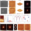
a SEM images of PDMS spiral patterns molded from the DLW 2D template (Supplementary Fig. 7c). The lengths of the white pointed lines in the SEM image represent physical distances of 200 nm and 500 nm, respectively. Scale bars are 3 μm and 500 nm for upper and lower images, respectively. b Scanning images respectively acquired by the CMA tip (a = 5 μm) and the solid tip (DLW solid cone) with images from left to right respectively corresponding to 2D height plots, 3D topographies, and 2D fast Fourier transformation (2D FFT) images of the height plots using a Hanning window. The same color bars are used for height, 3D topography, 2D FFT images, respectively. Scale bars are 3 μm for height and 3D topography images and 3 μm-1 for 2D FFT images. c Magnified surface details (scale bar is 500 nm) separately extracted from region A and B in the height plots of b. d Histogram analysis of interfacial landscape in c showing frequency counts (1 nm step) of height distribution. The histograms are fitted with Gaussian curves. e Height profiles along the white dash lines in b. f Boxplots of FWHM width and depth of the groove measured by the solid tip and CMA tip in b. The Boxplot marks the median (center line within box), the first and third quartile (box), and 1.5 times the interquartile range (whiskers). The corresponding data are exhibited as scatter plots on the right side of each box. g, h Height profile (g) of a flower pattern (Supplementary Fig. 7d, e) and the corresponding 2D FFT images (h) obtained by the CMA tip (a = 5 μm) and the solid tip (DLW solid cone) at a decreased setpoint value. i Imaging comparison using CMA tips with different unit side lengths (a = 5 μm and 2 μm). The surface grains are indicated with white and black arrows. Scale bars are 3 μm for g, i and 3 μm-1 for h. Source data of d–f are provided as a Source Data file.
Fig. 5
Fig. 5. AFM imaging of biosamples with RIE-etched CMA tip (a = 5 μm).
a, b Height and phase profiles of Shewanella oneidensis MR-1 bacterial cells subjected to repetitive scans by a commercial tip. c, d Height and phase profiles of Shewanella oneidensis MR-1 bacterial cells after repetitive scans of an RIE-etched CMA tip (a = 5 μm) (Supplementary Fig. 20). The scanning times are marked at the top right corner of each figure. e, f AFM imaging of fibroblasts with the etched CMA tip (a = 5 μm). Scale bars are 400 nm for ad and 5 μm for e, f.

Similar articles

Cited by

References

    1. Dufrene YF, et al. Imaging modes of atomic force microscopy for application in molecular and cell biology. Nat. Nanotechnol. 2017;12:295–307. doi: 10.1038/nnano.2017.45. - DOI - PubMed
    1. Jiang S, et al. Distinguishing adjacent molecules on a surface using plasmon-enhanced Raman scattering. Nat. Nanotechnol. 2015;10:865–869. doi: 10.1038/nnano.2015.170. - DOI - PubMed
    1. Knoll A, Magerle R, Krausch G. Tapping mode atomic force microscopy on polymers: where is the true sample surface. Macromolecules. 2001;34:4159–4165. doi: 10.1021/ma001311x. - DOI
    1. Alsteens D, Muller DJ, Dufrene YF. Multiparametric atomic force microscopy imaging of biomolecular and cellular systems. Acc. Chem. Res. 2017;50:924–931. doi: 10.1021/acs.accounts.6b00638. - DOI - PubMed
    1. Meng X, et al. Broad modulus range nanomechanical mapping by magnetic-drive soft probes. Nat. Commun. 2017;8:1944. doi: 10.1038/s41467-017-02032-y. - DOI - PMC - PubMed

Publication types

LinkOut - more resources