. 2020 Sep 3;7(22):2001662.
doi: 10.1002/advs.202001662. eCollection 2020 Nov.

Artificially Intelligent Tactile Ferroelectric Skin

Affiliations

Artificially Intelligent Tactile Ferroelectric Skin

Kyuho Lee et al. Adv Sci (Weinh). .

Abstract

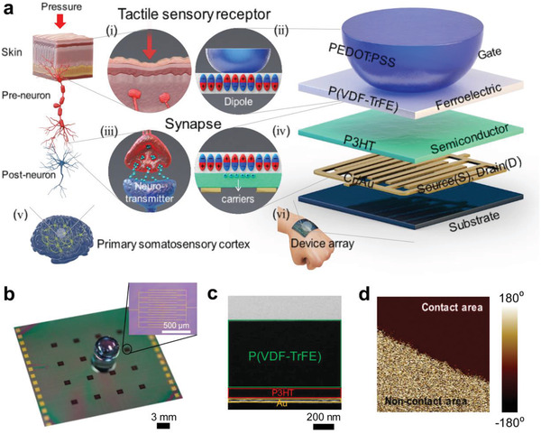
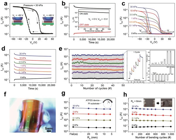
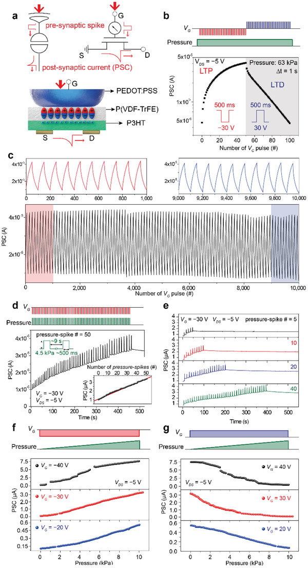
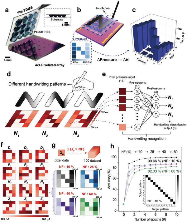
Lightweight and flexible tactile learning machines can simultaneously detect, synaptically memorize, and subsequently learn from external stimuli acquired from the skin. This type of technology holds great interest due to its potential applications in emerging wearable and human-interactive artificially intelligent neuromorphic electronics. In this study, an integrated artificially intelligent tactile learning electronic skin (e-skin) based on arrays of ferroelectric-gate field-effect transistors with dome-shape tactile top-gates, which can simultaneously sense and learn from a variety of tactile information, is introduced. To test the e-skin, tactile pressure is applied to a dome-shaped top-gate that measures ferroelectric remnant polarization in a gate insulator. This results in analog conductance modulation that is dependent upon both the number and magnitude of input pressure-spikes, thus mimicking diverse tactile and essential synaptic functions. Specifically, the device exhibits excellent cycling stability between long-term potentiation and depression over the course of 10 000 continuous input pulses. Additionally, it has a low variability of only 3.18%, resulting in high-performance and robust tactile perception learning. The 4 × 4 device array is also able to recognize different handwritten patterns using 2-dimensional spatial learning and recognition, and this is successfully demonstrated with a high degree accuracy of 99.66%, even after considering 10% noise.

Keywords: artificial tactile learning electronic‐skin; ferroelectric artificial synapses; ferroelectric‐gate field‐effect transistor sensing memory; tactile sensory synapses; wearable neuromorphic electronic devices.


Conflict of interest statement

The authors declare no conflict of interest.

Figures

Figure 1
Figure 1
Structure of ATFES device. a) Schematic of the biological tactile perception system: (i) the tactile sensory receptor, (iii) synapse, (v) primary somatosensory cortex in brain, and the corresponding artificial tactile learning e‐skin based on Fe‐FET device: (ii) artificial tactile reception system with dome‐shaped elastomeric gate electrode and ferroelectric layer below it, (iv) the artificial synapse has excess carriers corresponding to neurotransmitters that arise from ferroelectric dipoles, (vi) an array of artificial tactile learning devices on the skin which is equivalent to the cortex neural network. b) Photograph of 4 × 4  array of ATFES device with a pressure‐sensitive PEDOT:PSS gate electrodes. The inset is an optical microscope image of Au/P3HT/P(VDF‐TrFE) of an ATFES device. c) Cross‐sectional TEM image of an ATFES device, and d) PFM image of P(VDF‐TrFE) layer at the contact area boundary.
Figure 2
Figure 2
Switching and mechanical characterization of the ATFES. a) I DS –V G transfer curve showing current hysteresis stemmed from nonvolatile ferroelectric polarization of the P(VDF‐TrFE) layer. Pressure = 30 kPa.  b) The retention characteristic of ON and OFF states at V G = 0 V  and V DS = −5 V.  Inset: program/erase endurance up to 100 cycles. c) I DS –V G transfer curves at seven different pressures ranged from 0 to 30 kPa,  and d) the retention of each state at V G = 0 V  and V DS = −5 V.  The programming pressures and voltage (V G = −60 V)  were applied for 1 s. e) Repetitive multiple program/erase switching endurance test with seven different pressures. The inset shows a real‐time response, pressures sequence, and gate voltages sequence, respectively, for one cycle. After programmed or erased, I DS was read at V G = 0 V  and V DS = −5 V.  f) Photograph of a flexible ATFES array on the PI substrate, g) four distinct levels at V G = 0 programmed by V G = −60 V  as a function of R B, and h) bending endurance for the cycle test up to 1000 cycles under R B = 6 mm.  The inset photograph shows a flexible ATFES array in bent and unbent states.
Figure 3
Figure 3
Synaptic characteristics of the ATFES. a) Schematic of the signal transmission process between pre‐ and postneurons through the ATFES. The top insets show schematics of the tactile sensory receptor/synapse and corresponding circuit diagrams for the ATFES. b) LTP and LTD of the PSC as a function of the number of V G pulses of ±30 V  for 500 ms  at ≈63 kPa.  c) Cycling transition between the LTP and LTD for the ATFES during continuous 10 000 V G pulses. d) Plot of the PSC response at V DS = −5V  with respect to the 50 pressure‐spikes. Pressure = 4.5 kPa  and V G = −30 V  for ≈500 ms.  The inset shows the PSC level as a function of the number of pressure‐spikes. e) Plots of the PSC responses with respect to the different number of pressure‐spikes (ranging from 5 to 40). The reading and programming voltages and their sequences are the same as in (d). f) LTP and g) LTD of the PSC of the ATFES as functions of the magnitude of pressure (from 5 × 10−2 to 10 kPa)  and the V G (= ±20, ±30, and ±40 V) .
Figure 4
Figure 4
2‐dimensional spatial tactile mapping and handwriting pattern recognition of a 4 × 4 ATFES array. a) Photograph of 4 × 4 pixelated ATFES array combined with dome‐shaped PEDOT:PSS gate electrodes on the flat PDMS. The inset shows a cross‐sectional photograph of the ATFES array. b) Schematic illustration of the alphabet “N” pattern written by a commercial touch pen on the 4 × 4 ATFES array. Inset shows the “N” pattern encoded by the different magnitude of pressure‐spike (from 5×10 −2 to 40kPa)  at VG = −30V.  c) The histogram of Δw/wo in the 4 × 4 ATFES array. d) Schematic illustrations of three different handwriting styles for the “N” patterns (N1, N2, and N3). The bottom inset shows the contour plot of corresponded PSC levels as examples. e) Constituents of a single‐layer neural network for the handwriting pattern recognition. f) The contour plots of the measured PSC levels for four alphabet characters (“D,” “P,” “N,” “Z”) encoded by three different handwriting styles (1, 2, 3). g) Examples of four “N3” pattern dataset were generated by different NF values (10%, 25%, 40%, and 60%). h) Recognition accuracy for the handwriting patterns during 10 learning epochs with different NF values. Inset shows the confusion matrices between the output and target patterns for a classification test of 12 alphabetical character sets for NF = 10%.

References

    1. Mannsfeld S. C. B., Tee B. C. K., Stoltenberg R. M., Chen C. V. H. H., Barman S., Muir B. V. O., Sokolov A. N., Reese C., Bao Z., Nat. Mater. 2010, 9, 859. - PubMed
    1. Schwartz G., Tee B. C. K., Mei J., Appleton A. L., Kim D. H., Wang H., Bao Z., Nat. Commun. 2013, 4, 1859. - PubMed
    1. Lee S., Reuveny A., Reeder J., Lee S., Jin H., Liu Q., Yokota T., Sekitani T., Isoyama T., Abe Y., Suo Z., Someya T., Nat. Nanotechnol. 2016, 11, 472. - PubMed
    1. Gao Y., Ota H., Schaler E. W., Chen K., Zhao A., Gao W., Fahad H. M., Leng Y., Zheng A., Xiong F., Zhang C., Tai L. C., Zhao P., Fearing R. S., Javey A., Adv. Mater. 2017, 29, 1701985. - PubMed
    1. Bae G. Y., Han J. T., Lee G., Lee S., Kim S. W., Park S., Kwon J., Jung S., Cho K., Adv. Mater. 2018, 30, 1803388. - PubMed

LinkOut - more resources