. 2020 Dec 14;10(1):21888.
doi: 10.1038/s41598-020-78837-7.

Enhanced image sensing with avalanche multiplication in hybrid structure of crystalline selenium photoconversion layer and CMOSFETs

Affiliations

Enhanced image sensing with avalanche multiplication in hybrid structure of crystalline selenium photoconversion layer and CMOSFETs

Shigeyuki Imura et al. Sci Rep. .

Abstract

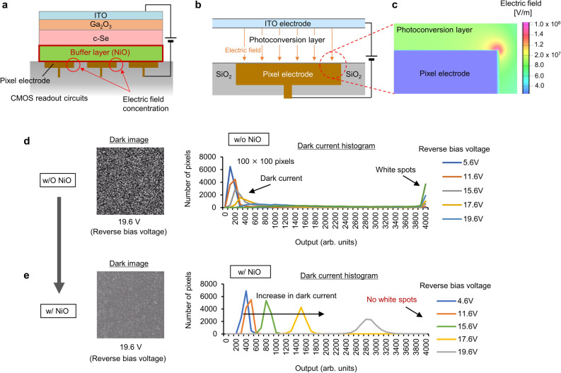
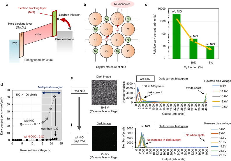
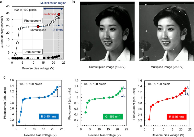
The recent improvements of complementary metal-oxide-semiconductor (CMOS) image sensors are playing an essential role in emerging high-definition video cameras, which provide viewers with a stronger sensation of reality. However, the devices suffer from decreasing sensitivity due to the shrinkage of pixels. We herein address this problem by introducing a hybrid structure comprising crystalline-selenium (c-Se)-based photoconversion layers and 8 K resolution (7472 × 4320 pixels) CMOS field-effect transistors (FETs) to amplify signals using the avalanche multiplication of photogenerated carriers. Using low-defect-level NiO as an electric field buffer and an electron blocking layer, we confirmed signal amplification by a factor of approximately 1.4 while the dark current remained low at 2.6 nA/cm2 at a reverse bias voltage of 22.6 V. Furthermore, we successfully obtained a brighter image based on the amplified signals without any notable noise degradation.


Conflict of interest statement

The authors declare no competing interests.

Figures

Figure 1
Figure 1
Device structure and pixel configuration. (a) Schematic cross section of the stacked CMOS image sensor with detailed photoconversion layer information. (b) Cross-sectional scanning electron microscopy image of a pixel. (c) Cross-sectional transmission electron microscopy image of a photoconversion layer. (d) Schematic diagram of a pixel. (e) Block diagram and photomicrograph of the chip.
Figure 2
Figure 2
Electric field relaxation effects of NiO buffer layer. (a) Schematic of the electric field relaxation effects of NiO buffer layer. (b) Schematic cross-sectional illustration of the pixel model and c mapping of the calculated electric field gradient around a pixel electrode at an applied voltage of 3 V. Dark images (100 × 100 pixels) and their histograms with different reverse bias voltages captured by the stacked CMOS image sensors overlaid with photoconversion layers (d) without and (e) with NiO buffer layers, respectively.
Figure 3
Figure 3
Effects of NiO electron blocking layer on dark current reduction. (a) Schematic of the effects of a NiO electron blocking layer on preventing electron injection from an external electrode. (b) Schematic diagram of the crystal structure of NiO with Ni vacancies. (c) Comparison of relative dark current of the test devices on glass substrates consisting of photoconversion layers without NiO and with NiO (O2 fractions of 10% and 3%). (d) Dark current density of the photoconversion layers with and without NiO (O2 fraction of 3%) on the CMOS readout circuits as a function of reverse bias voltage measured at room temperature. Dark images (100 × 100 pixels) and their histograms with different reverse bias voltages captured by the stacked CMOS image sensors overlaid with photoconversion layers (e) without and (f) with NiO (O2 fraction of 3%) electron blocking layers, respectively.
Figure 4
Figure 4
Electric field relaxation effects of NiO buffer layer. (a) Current density–voltage characteristics of a photoconversion layer with NiO (O2 fraction of 3%) stacked onto the CMOS readout circuit, in the dark and illuminated through a blue filter. (b) Partial images extracted from the original 8 K images captured by the stacked CMOS image sensors at reverse bias voltages of 12.6 V (unmultiplied) and 22.6 V (multiplied). (c) Normalized photocurrent–voltage characteristics of the stacked CMOS image sensors for the illuminated conditions through the blue, green, and red filters.

References

    1. Hasegawa T, et al. A new 0.8µm CMOS image sensor with low RTS noise and high full well capacity. IISW Dig. Tech. Pap. 2019;1:24–27.
    1. Okawa T, et al. A 1/2inch 48M all PDAF CMOS image sensor using 0.8µm Quad Bayer coding 2×2OCL with 1.0lux minimum AF illuminance level. IEDM Dig. Tech. Pap. 2019;1:1631–1634.
    1. Kim HC, et al. A ½.65 in 44Mpixel CMOS image sensor with 0.7 µm pixels fabricated in advanced full-depth deep-trench isolation technology. ISSCC Dig. Tech. Pap. 2020;1:104–106.
    1. Tanioka K, et al. An avalanche-mode amorphous selenium photoconductive layer for use as a camera tube target. IEEE Electron. Device Lett. 1987;8:392–394. doi: 10.1109/EDL.1987.26671. - DOI
    1. Mcintyre RJ. Multiplication noise in uniform avalanche diodes. IEEE Trans. Electron. Devices. 1966;13:164–168. doi: 10.1109/T-ED.1966.15651. - DOI