. 2020 Dec 17;11(1):6404.
doi: 10.1038/s41467-020-20115-1.

Zero-bias mid-infrared graphene photodetectors with bulk photoresponse and calibration-free polarization detection

Affiliations

Zero-bias mid-infrared graphene photodetectors with bulk photoresponse and calibration-free polarization detection

Jingxuan Wei et al. Nat Commun. .

Abstract

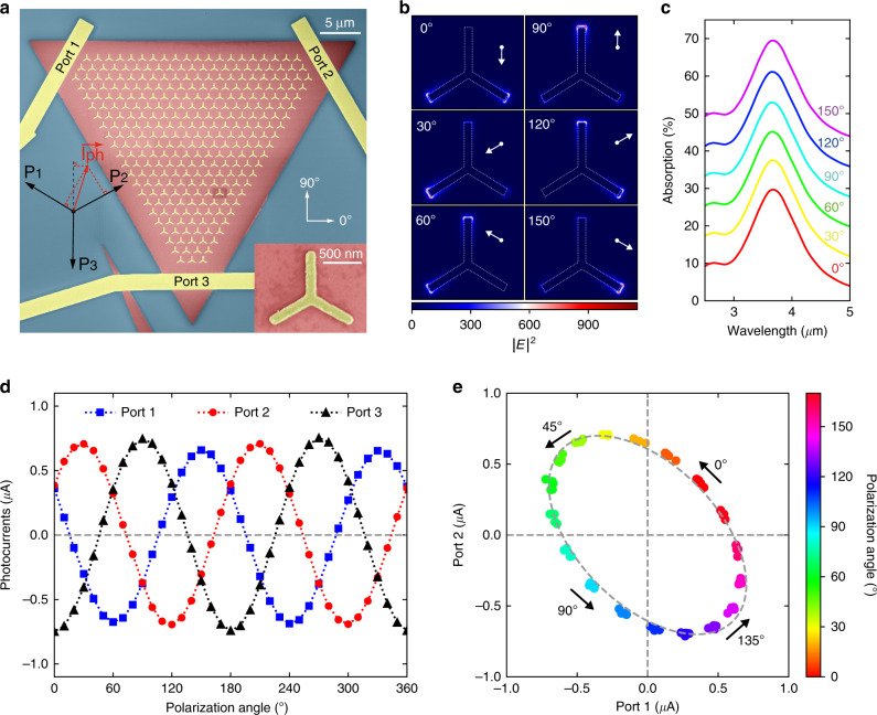
Bulk photovoltaic effect (BPVE), featuring polarization-dependent uniform photoresponse at zero external bias, holds potential for exceeding the Shockley-Queisser limit in the efficiency of existing opto-electronic devices. However, the implementation of BPVE has been limited to the naturally existing materials with broken inversion symmetry, such as ferroelectrics, which suffer low efficiencies. Here, we propose metasurface-mediated graphene photodetectors with cascaded polarization-sensitive photoresponse under uniform illumination, mimicking an artificial BPVE. With the assistance of non-centrosymmetric metallic nanoantennas, the hot photocarriers in graphene gain a momentum upon their excitation and form a shift current which is nonlocal and directional. Thereafter, we demonstrate zero-bias uncooled mid-infrared photodetectors with three orders higher responsivity than conventional BPVE and a noise equivalent power of 0.12 nW Hz-1/2. Besides, we observe a vectorial photoresponse which allows us to detect the polarization angle of incident light with a single device. Our strategy opens up alternative possibilities for scalable, low-cost, multifunctional infrared photodetectors.


Conflict of interest statement

The authors declare no competing interests.

Figures

Fig. 1
Fig. 1. Design concept and main results of metasurface-mediated graphene photodetectors.
a Illustration of the designed metasurface-mediated graphene photodetector, which consists of non-centrosymmetric sub-wavelength metallic nanoantennas as meta-atoms on top of graphene flakes. Under uniform illumination at 4 µm wavelength, global directional photocurrents are generated from each meta-atom at zero external bias (Vd = Vg = 0 V), mimicking the shift current in the bulk photovoltaic effect (BPVE). Importantly, due to the gapless nature of graphene, the local photoresponse from nanoantennas can efficiently contribute to the external circuit in a nonlocal manner, enabling a cascaded total photocurrent. From bottom to top: Si (gray), SiO2 (blue), graphene (black honeycomb), Pd/Au for nanoantennas, and electrodes (yellow). Inset illustrates the excitation of electrons at one edge of nanoantennas and the following directional transport. Black line denotes the band diagram of graphene. Yellow area is the graphene region that is covered and doped by metal. b Schematic of the experimental setup with control of the linear polarization state via rotation of half-wave plate (HWP). The focused laser beam has a beam diameter around 400 μm, which is much larger than the size of our device. The inset shows the scanning electron microscopy (SEM) image of our device in false colors: graphene in dark red, nanoantennas, and electrodes in yellow, substrate in dark blue. c Simulated near-field distribution and predicted vectorial photocurrent in a unit cell at different polarization angles of incident light (Pol). |E|2 represents the intensity of local electrical field. Yellow wave arrows indicate the flow of photocarriers generated at the nanoantenna–graphene interfaces. White arrows illustrate the resultant vectorial photocurrents (Iph). d Polar plot of measured Iph, which is the scalar projection of Iph on the orientation of drain–source electrodes. Red and blue areas mark the positive and negative signs of Iph.
Fig. 2
Fig. 2. Evidence of bulk photoresponse.
a, b SEM images and measured photovoltage of three devices with different degrees of asymmetry. When the lengths of horizontal arms (Lh) decrease from device C to A, the photoresponse decreases and vanishes eventually due to the absence of broken symmetry. c, d SEM images and measured photovoltage of five devices with different numbers of nanoantennas, where the nanoantennas closest to the contact electrodes are removed gradually from Device D′ to A′. Device E′ has the same number of nanoantennas as device D′, but the orientation of nanoantennas is reversed. The photovoltages is only dependent on the number of nanoantennas but insensitive to their position. The non-zero photoresponse of device A′ could be due to non-uniform illumination, fabrication imperfections or nonlocal photoresponse from neighboring devices. Error bars are smaller than the size of markers. Dashed lines are guides to the eye.
Fig. 3
Fig. 3. Device characterization.
a Measured photovoltage during on-off cycles of an incident laser at 4 μm wavelength. Light is modulated with an optical chopper at 800 Hz. b Measured currents versus applied Vd at dark and light conditions, with their difference as the photocurrents. 0° and 90° denote the polarization angles of the incident light. The intersections with x and y axes represent open-circuit voltage and short-circuit current, respectively. c Measured photocurrent versus gate voltage at 0° and 90° polarization angles. Inset shows the respective band diagrams. While the Fermi level of the graphene covered by nanoantennas (yellow region) is pinned, the Fermi level of uncovered graphene channel can be tuned by gate voltage, leading to flipping of band bending and hence opposite photoresponse. d Measured and predicted frequency response. Red shaded area denotes the range of reported data and hence the uncertainty of our estimation. e Dependence of photocurrents on the power of incident light at two different gate voltages. The polarization angle is 0°. f Measured frequency-dependent noises and calculated noise equivalent power (NEP). The similar trend between noise and NEP is due to the almost constant frequency responsivity. Johnson noise becomes dominant for frequencies above 1 kHz.
Fig. 4
Fig. 4. Calibration-free polarization detection.
a SEM images of a three-port device for calibration-free polarization detection. The bottom left inset shows how the Iph is decomposed into the currents measured at the three ports. The scalar projection is valid in our case because of the three-fold rotation symmetry. Bottom right inset shows the zoom-in graph of a single triangle nanoantenna. b Simulated near-field distribution of the half unit cell and predicted direction of photocurrent at different polarization angles (θ). c Far-field absorption spectra of metasurface, which show no dependence on the polarization angle due to the three-fold rotation symmetry. The spectra have been shifted vertically for better clarity. d Measured photocurrent at the three ports as a function of polarization angles. No external bias is applied. The results can be well fitted with P1~cos(2θ + π/3), P2~cos(2θ−π/3), P3~cos(2θ−π). e Two-dimensional plot of P1 and P2. By sweeping the polarization angle, (P1, P2) pairs form a closed curve that fulfills the equation of an ellipse. The light intensity and polarization can then be decoupled, enabling an unambiguous detection of the polarization state using a single device.

References

    1. Liu J, Xia F, Xiao D, García de Abajo FJ, Sun D. Semimetals for high-performance photodetection. Nat. Mater. 2020;19:830–837. doi: 10.1038/s41563-020-0715-7. - DOI - PubMed
    1. Koppens FHL, et al. Photodetectors based on graphene, other two-dimensional materials and hybrid systems. Nat. Nanotechnol. 2014;9:780–793. doi: 10.1038/nnano.2014.215. - DOI - PubMed
    1. Spanier JE, et al. Power conversion efficiency exceeding the Shockley–Queisser limit in a ferroelectric insulator. Nat. Photonics. 2016;10:611–616. doi: 10.1038/nphoton.2016.143. - DOI
    1. Dhara S, Mele EJ, Agarwal R. Voltage-tunable circular photogalvanic effect in silicon nanowires. Science. 2015;349:726–729. doi: 10.1126/science.aac6275. - DOI - PubMed
    1. Zhang YJ, et al. Enhanced intrinsic photovoltaic effect in tungsten disulfide nanotubes. Nature. 2019;570:349–353. doi: 10.1038/s41586-019-1303-3. - DOI - PubMed