Review
. 2020 Nov 10;7(24):2002697.
doi: 10.1002/advs.202002697. eCollection 2020 Dec.

2D Materials and Heterostructures at Extreme Pressure

Affiliations
Review

2D Materials and Heterostructures at Extreme Pressure

Linglong Zhang et al. Adv Sci (Weinh). .

Abstract

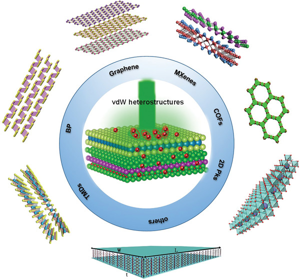
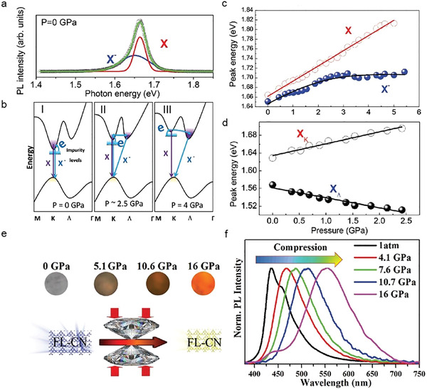
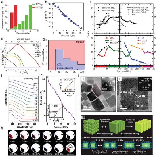
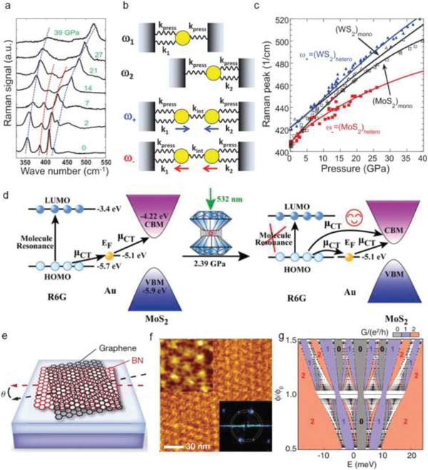
2D materials possess wide-tuning properties ranging from semiconducting and metallization to superconducting, etc., which are determined by their structure, empowering them to be appealing in optoelectronic and photovoltaic applications. Pressure is an effective and clean tool that allows modifications of the electronic structure, crystal structure, morphologies, and compositions of 2D materials through van der Waals (vdW) interaction engineering. This enables an insightful understanding of the variable vdW interaction induced structural changes, structure-property relations as well as contributes to the versatile implications of 2D materials. Here, the recent progress of high-pressure research toward 2D materials and heterostructures, involving graphene, boron nitride, transition metal dichalcogenides, 2D perovskites, black phosphorene, MXene, and covalent-organic frameworks, using diamond anvil cell is summarized. A detailed analysis of pressurized structure, phonon dynamics, superconducting, metallization, doping together with optical property is performed. Further, the pressure-induced optimized properties and potential applications as well as the vision of engineering the vdW interactions in heterostructures are highlighted. Finally, conclusions and outlook are presented on the way forward.

Keywords: 2D materials; diamond anvil cell (DAC); high pressure; metallization; optoelectronics; superconducting.


Conflict of interest statement

The authors declare no conflict of interest.

Figures

Figure 1
Figure 1
Schematic illustration of several common 2D materials.
Figure 2
Figure 2
Common crystal structures of various TMD phases. Reproduced with permission.[ 55 ] Copyright 2020, Annual Reviews, Inc.
Figure 3
Figure 3
High‐pressure technique. a) Schematic of common diamond anvil cell (DAC). b) Phase diagram of carbon. Reproduced with permission.[ 142 ] Copyright 2020, Wikimedia Foundation.
Figure 4
Figure 4
Tuning of structures under high pressure. a) Resistivity as a function of pressure in MoS2. b) The relative energy of MoTe2, MoSe2, and MoS2 as a function of relative sliding ranging from 2Hc to 2Ha. c–f) Theoretical band structure as a function of pressure under ambient pressure, 23 GPa, 41 GPa, and 58 GPa, respectively. g) Crystal structures from various allotropes of phosphorus under different pressure. a) Reproduced with permission.[ 19 ] Copyright 2014, Springer Nature. b–f) Reproduced with permission.[ 20 ] Copyright 2015, Springer Nature. g) Reproduced with permission.[ 32 ] Copyright 2017, American Physical Society.
Figure 5
Figure 5
Phonon dynamics under high pressure. a,b) Raman spectra of monolayer 2H‐MoS2 and 1T′ MoS2 under the indicated pressure. It shows the pressure‐dependent phonon dynamics of different‐phase MoS2 monolayer. c) FWHM evolutions as a function of pressure from BP. The vertical dashed lines represent the pressure points of the structural phase transitions. d) FWHM evolutions of BP under pressure ranging from 0 to 4 GPa. e) Raman spectra of 2D perovskite (PEA)2PbI4 under the indicated pressure. f) Raman peak position evolution of Peak 1 during the compression and decompression. a,b) Reproduced with permission.[ 18 ] Copyright 2014, American Chemical Society. c,d) Reproduced with permission.[ 33 ] Copyright 2017, American Physical Society. e,f) Reproduced with permission.[ 39 ] Copyright 2017, American Association for the Advancement of Science.
Figure 6
Figure 6
Pressure‐induced metallization. a) Temperature–pressure contour plot of resistivity under various pressure, showing the phase transition from semiconducting to the metallic state. b) Arrhenius curve demonstrating the emergence of the metallic phase at a pressure beyond 22 GPa. c) Calculated band structure at 0, 20.4, and 39.5 GPa, showing that the bandgap approaches zero with the increase of pressure. Moreover, a complete metallization was observed at 39.5 GPa. d,e) The calculated band structures of 2D VS2: under ambient pressure and 18.68 GPa. a–c) Reproduced with permission.[ 17 ] Copyright 2015, American Chemical Society. d,e) Reproduced with permission.[ 11 ] Copyright 2017, Wiley‐VCH.
Figure 7
Figure 7
Pressure‐induced superconductivity. a) Pressure‐dependent isothermal resistance of ReS2 at 5, 100, and 200 K. b) Magnetic field‐dependent resistance at 102 GPa. The upper critical field µ 0 H c2 is presented in the inset. The experimental data are fitted by the Ginzburg–Landau (GL) formula. c) Pressure–temperature (P–T) phase diagram of 2H‐MoS2, demonstrating the respective regions of superconducting and metallic phases. d) Theoretical XRD spectra at 10 GPa together with experimental data at the indicated condition. e,f) Experimental XRD spectra showing clear splittings in the peaks of (011) and (113), demonstrating the occurrence of phase transitions. a,b) Reproduced with permission.[ 167 ] Copyright 2017, Springer Nature. c) Reproduced with permission.[ 113 ] Copyright 2018, American Physical Society. d–f) Reproduced with permission.[ 184 ] Copyright 2016, American Physical Society.
Figure 8
Figure 8
Pressure‐induced doping. a–c) Schematic diagram of the transition process for neutral exciton (X0) and trions (X) in 2H‐MoSe2 monolayer, peak position evolutions of X0 and X versus pressure, and the PL intensity ratio of X0 to X as a function of pressure, respectively.[ 46 ] d,e) Calculated electronic structure at ambient pressure and 3 GPa. f) The Dirac point (left axis) and the induced carrier density (right axis) of graphene from the heterostructure of graphene/MoS2 versus pressure. a–c) Reproduced with permission.[ 46 ] Copyright 2017, American Chemical Society. d–f) Reproduced with permission.[ 37 ] Copyright 2016, Wiley‐VCH.
Figure 9
Figure 9
Pressure tuned optical properties. a) PL spectra of 1L WSe2 at ambient pressure. b) The band structure of 1L WSe2 at 0 GPa (I), around 2.25 GPa (II), and 4 GPa (III), respectively. c) Photon energy of X and X exciton peaks as a function of pressure in 1L WSe2. d) Photon energy of X and X exciton peaks as a function of pressure in 2L WSe2. e) Schematic illustration of PL emission color for FL‐CN samples under different pressures. f) Normalized PL spectra of FL‐CN samples at the indicated pressures. a–d) Reproduced with permission.[ 221 ] Copyright 2016, Royal Society of Chemistry. e,f) Reproduced with permission.[ 220 ] Copyright 2020, Royal Society of Chemistry.
Figure 10
Figure 10
Optimized optoelectronic properties. a) The calculated bandgap change of T‐ and H‐ZrTe2 with the increase of pressure.[ 201 ] b) Resistivity as a function of pressure for MoSe2. c) Bandgap changes versus pressure in various MoS2 polytypes. d) Pressure‐induced phase transitions in various MoS2 polytypes. e) Several experimental and calculated critical temperature (T c) of phosphorus under high pressure. f) Pressure‐dependent UV–vis absorption spectra of 2D Cs3Sb2I9 perovskite. g) The pressure‐dependent bandgap of 2D Cs3Sb2I9, where the inset describes the bandgap Tauc plots at 0 and 20 GPa. h) Optical images of 2D Cs3Sb2I9 under various pressures. i) Pressure‐induced synthesis of 2D CsPbBr3 perovskite nanoplates. a) Reproduced with permission.[ 201 ] Copyright 2015, Royal Society of Chemistry. b) Reproduced with permission.[ 20 ] Copyright 2015, Springer Nature. c,d) Reproduced with permission.[ 18 ] Copyright 2014, American Chemical Society. e) Reproduced with permission.[ 32 ] Copyright 2017, American Physical Society. f–h) Reproduced with permission.[ 43 ] Copyright 2020, Royal Society of Chemistry. i) Reproduced with permission.[ 226 ] Copyright 2017, Wiley‐VCH.
Figure 11
Figure 11
Engineering vdW interactions. a) Pressure‐dependent Raman spectra of WS2/MoS2 bilayers (the dashed lines are for guiding the eyes). b) Schematic modeling two coupled harmonic oscillators, where ω± and k int represent the renormalized vibration frequencies and the enhanced coupling, respectively. The arrows reveal the vibration directions, which correspond to the optical‐like and acoustic‐like modes. c) The model fitting of A′1 modes in heterostructures [(WS2)hetero (blue) and (MoS2)hetero (red)]. (WS2)mono and (MoS2)mono stand for the A′1 modes of the individual TMDs. d) Surface‐enhanced Raman spectroscopy (SERS) charge transfer process in a system of MoS2/Au/R6G. e) Schematic of graphene stacking on h‐BN with an angle of θ, showing the occurrence of Moiré patterns. f) The measured Moiré patterns of graphene/h‐BN with a triangular lattice, where the upper inset demonstrates the enlarged image and the lower inset is a fast Fourier transfer of the measured regions, showing the Moiré wavelength of 15.5 ± 0.9 nm. g) Calculated Hofstadter energy spectrum of the full spin and sublattice‐spin N = 0 Landau level. The dense energy bands are described by the black points; the interval spectral gaps are coded with different color, which represents the corresponding two‐terminal conductance: 2 (red), 1 (purple), and 0 (gray). a–c) Reproduced with permission.[ 235 ] Copyright 2015, American Physical Society. d) Reproduced with permission.[ 45 ] Copyright 2015, Royal Society of Chemistry. e,f) Reproduced with permission.[ 258 ] Copyright 2015, Springer Nature. g) Reproduced with permission.[ 257 ] Copyright 2013, the American Association for the Advancement of Science.

References

    1. Novoselov K. S., Mishchenko A., Carvalho A., Castro Neto A. H., Science 2016, 353, aac9439. - PubMed
    1. Novoselov K. S., Fal'Ko V. I., Colombo L., Gellert P. R., Schwab M. G., Kim K., Nature 2012, 490, 192. - PubMed
    1. Wang Y., Kim J. C., Wu R. J., Martinez J., Song X., Yang J., Zhao F., Mkhoyan A., Jeong H. Y., Chhowalla M., Nature 2019, 568, 70. - PubMed
    1. Novoselov K., Nat. Mater. 2007, 6, 720. - PubMed
    1. Xia F., Wang H., Xiao D., Dubey M., Ramasubramaniam A., Nat. Photonics 2014, 8, 899.

LinkOut - more resources