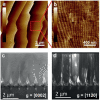
Sec-Eliminating the SARS-CoV-2 by AlGaN Based High Power Deep Ultraviolet Light Source
- PMID: 33349747
- PMCID: PMC7744859
- DOI: 10.1002/adfm.202008452
Sec-Eliminating the SARS-CoV-2 by AlGaN Based High Power Deep Ultraviolet Light Source
Abstract
The world-wide spreading of coronavirus disease (COVID-19) has greatly shaken human society, thus effective and fast-speed methods of non-daily-life-disturbance sterilization have become extremely significant. In this work, by fully benefitting from high-quality AlN template (with threading dislocation density as low as ≈6×108 cm-2) as well as outstanding deep ultraviolet (UVC-less than 280 nm) light-emitting diodes (LEDs) structure design and epitaxy optimization, high power UVC LEDs and ultra-high-power sterilization irradiation source are achieved. Moreover, for the first time, a result in which a fast and complete elimination of SARS-CoV-2 (the virus causes COVID-19) within only 1 s is achieved by the nearly whole industry-chain-covered product. These results advance the promising potential in UVC-LED disinfection particularly in the shadow of COVID-19.
Keywords: AlGaN based device; SARS‐CoV‐2; fast sterilization; ultraviolet C LED.
© 2020 Wiley‐VCH GmbH.
Conflict of interest statement
The authors declare no conflict of interest.
Figures


Similar articles
-
Effects of GaN/AlGaN/Sputtered AlN nucleation layers on performance of GaN-based ultraviolet light-emitting diodes.Sci Rep. 2017 Mar 15;7:44627. doi: 10.1038/srep44627. Sci Rep. 2017. PMID: 28294166 Free PMC article.
-
UV Inactivation of SARS-CoV-2 across the UVC Spectrum: KrCl* Excimer, Mercury-Vapor, and Light-Emitting-Diode (LED) Sources.Appl Environ Microbiol. 2021 Oct 28;87(22):e0153221. doi: 10.1128/AEM.01532-21. Epub 2021 Sep 8. Appl Environ Microbiol. 2021. PMID: 34495736 Free PMC article.
-
Highly efficient AlGaN-based deep-ultraviolet light-emitting diodes: from bandgap engineering to device craft.Microsyst Nanoeng. 2024 Aug 13;10:110. doi: 10.1038/s41378-024-00737-x. eCollection 2024. Microsyst Nanoeng. 2024. PMID: 39145147 Free PMC article.
-
COVID-19 pandemic lesson learned- critical parameters and research needs for UVC inactivation of viral aerosols.J Hazard Mater Adv. 2022 Nov;8:100183. doi: 10.1016/j.hazadv.2022.100183. Epub 2022 Oct 12. J Hazard Mater Adv. 2022. PMID: 36619826 Free PMC article. Review.
-
AlGaN-based ultraviolet light-emitting diodes: challenges and opportunities.Luminescence. 2021 Mar;36(2):294-305. doi: 10.1002/bio.3965. Epub 2020 Nov 15. Luminescence. 2021. PMID: 33075209 Review.
Cited by
-
UVC, UVB and UVA susceptibility of Phi6 and its suitability as a SARS-CoV-2 surrogate.AIMS Microbiol. 2022 Jul 8;8(3):278-291. doi: 10.3934/microbiol.2022020. eCollection 2022. AIMS Microbiol. 2022. PMID: 36317004 Free PMC article.
-
The Structural Evolution of Semipolar (11-22) Plane AlN Tem-Plate on m-Plane Sapphire Prepared by Sputtering and High Temperature Annealing.Materials (Basel). 2022 Apr 18;15(8):2945. doi: 10.3390/ma15082945. Materials (Basel). 2022. PMID: 35454640 Free PMC article.
-
Reduction of parasitic reaction in high-temperature AlN growth by jet stream gas flow metal-organic vapor phase epitaxy.Sci Rep. 2022 May 10;12(1):7662. doi: 10.1038/s41598-022-10937-y. Sci Rep. 2022. PMID: 35538125 Free PMC article.
-
Ultrafast-UV laser integrating cavity device for inactivation of SARS-CoV-2 and other viruses.Sci Rep. 2022 Jul 13;12(1):11935. doi: 10.1038/s41598-022-13670-8. Sci Rep. 2022. PMID: 35831374 Free PMC article.
-
A Comprehensive Review of Group-III Nitride Light-Emitting Diodes: From Millimeter to Micro-Nanometer Scales.Micromachines (Basel). 2024 Sep 25;15(10):1188. doi: 10.3390/mi15101188. Micromachines (Basel). 2024. PMID: 39459062 Free PMC article. Review.
References
-
- Ogata N., Sakasegawa M., Miura T., Shibata T., Takigawa Y., Taura K., Taguchi K., Matsubara K., Nakahara K., Kato D., Sogawa K., Oka H., Pharmacology 2016, 97, 301. - PubMed
-
- Abbasi R., Jain R., Nelson K., Busche D., Lynn D. M., Abbott N. L., Adv. Funct. Mater. 2019, 29, 1804851.
-
- Ruiz‐Hitzky E., Darder M., Wicklein B., Ruiz‐Garcia C., Martín‐Sampedro R., del Real G., Aranda P., Adv. Healthcare Mater. 2020, 9, 2000979. - PubMed
-
- Garcia de Abajo F. J., Hernandez R. J., Kaminer I., Meyerhans A., Rosell‐Llompart J., Sanchez‐Elsner T., ACS Nano 2020, 14, 7704. - PubMed
LinkOut - more resources
Full Text Sources
Miscellaneous
