Review
. 2020 Nov 19;8(1):2002418.
doi: 10.1002/advs.202002418. eCollection 2020 Jan.

Recent Progress in Organic Photodetectors and their Applications

Affiliations
Review

Recent Progress in Organic Photodetectors and their Applications

Hao Ren et al. Adv Sci (Weinh). .

Abstract

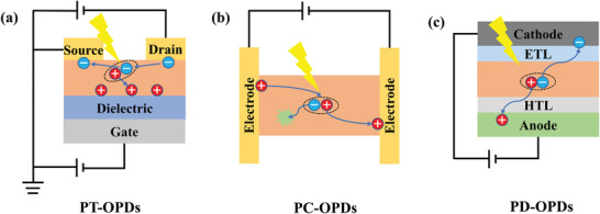
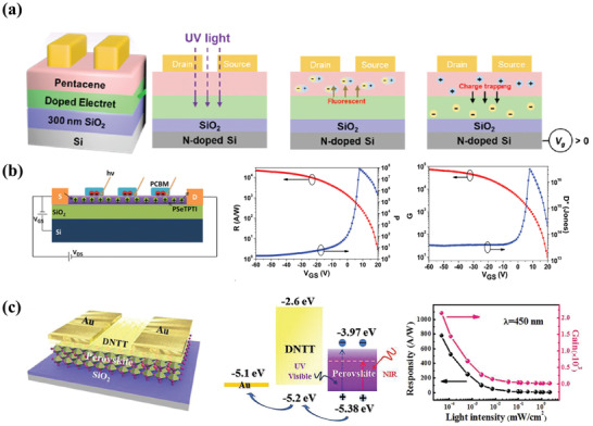
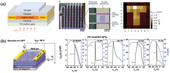
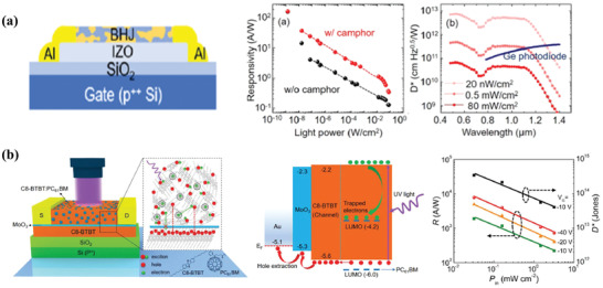
Organic photodetectors (OPDs) have attracted continuous attention due to their outstanding advantages, such as tunability of detecting wavelength, low-cost manufacturing, compatibility with lightweight and flexible devices, as well as ease of processing. Enormous efforts on performance improvement and application of OPDs have been devoted in the past decades. In this Review, recent advances in device architectures and operation mechanisms of phototransistor, photoconductor, and photodiode based OPDs are reviewed with a focus on the strategies aiming at performance improvement. The application of OPDs in spectrally selective detection, wearable devices, and integrated optoelectronics are also discussed. Furthermore, some future prospects on the research challenges and new opportunities of OPDs are covered.

Keywords: detection; flexibility; integrated optoelectronics; organic photodetectors; photomultiplication effect.


Conflict of interest statement

The authors declare no conflict of interest.

Figures

Figure 1
Figure 1
Schematic working mechanisms of a) PT‐OPDs, b) PC‐OPDs, and c) PD‐OPDs.
Figure 2
Figure 2
a) Schematic device structure and operation mechanism of PT‐OPDs. Reproduced with permission.[ 26 ] Copyright 2019, The Royal Society of Chemistry. b) Schematic device structure, along with photoresponsivity and detectivity as a function of V GS. Reproduced with permission.[ 27 ] Copyright 2015, Wiley‐VCH. c) Schematic device structure and operation mechanism of the hybrid PT‐OPDs, along with responsivity and gain as a function of incident light intensity. Reproduced with permission.[ 21 ] Copyright 2019, Wiley‐VCH.
Figure 3
Figure 3
a) Schematic device structure of dual‐gate PT‐OPDs, an optical micrograph of the detector array, and the detected image. Reproduced under the terms of the CC‐BY 4.0 international license.[ 32 ]Copyright 2018, The Authors. Published by Springer Nature. b) Schematic diagram of the device structure, photosensitivity, and photoresponsivity of PI1:C5BTBT PT‐OPDs. Reproduced with permission.[ 33 ] Copyright 2017, Wiley‐VCH.
Figure 4
Figure 4
a) Phototransistor structure with indium zinc oxide (IZO) as an electron transporting layer. Photoresponsivity and detectivity as a function of incident light power. Reproduced with permission.[ 34 ] Copyright 2019, American Chemical Society. b) Schematic device structure, energy level diagram, and photoresponsivity as a function of power intensity for hybrid‐layered PT‐OPDs. Reproduced with permission.[ 35 ] Copyright 2019, Wiley‐VCH.
Figure 5
Figure 5
a) Schematic device structure and EQE spectrum of a NIR photoconductor. Reproduced with permission.[ 39 ] Copyright 2015, The Royal Society of Chemistry. b) Schematic device structure, external photoconductive gain, and photoresponsivity of the doped photoconductor. Reproduced under the terms of the CC‐BY 4.0 international license.[ 19 ] Copyright 2019, The Authors. Published by Springer Nature.
Figure 6
Figure 6
a) Schematic device structure, energy diagram, and gain dependency versus frequency with different trap concentrations of PC‐OPDs.Reproduced with permission.[ 52 ] Copyright 2020, AIP Publishing. b) Schematic device structure and work mechanism of hybrid PD‐OPDs. Reproduced with permission.[ 54 ] Copyright 2014, Wiley‐VCH.
Figure 7
Figure 7
Schematic diagram of planar heterojunction and bulk heterojunction.
Figure 8
Figure 8
a) Schematic device structure of the photodetector with ZnO nanoparticles mixed in the C‐TPD buffer layer. b) EQE spectra of the photodetector under reverse bias from 0 to −8 V with a voltage step of 1 V. c) Energy level diagram of the reverse‐biased photodetector in dark and under illumination. Reproduced with permission.[ 79 ] Copyright 2014, Wiley‐VCH.
Figure 9
Figure 9
a) The relative band energies of the device with and without illumination. Reproduced with permission.[ 82 ] Copyright 2017, Wiley‐VCH. b) Schematic band structure of the interfacial band bending in PM type OPDs under the different situations of illumination and bias. Reproduced with permission.[ 85 ] Copyright 2020, The Royal Society of Chemistry.
Figure 10
Figure 10
a) Device structure, active layer materials structure, and energy band diagram of UV photodetectors. Illustration of the device in dark under b) forward bias and c) reverse bias. Illustration of the device with illumination under d) forward bias and e) reverse bias. f) EQE spectra of the device under different forward bias. Reproduced with permission.[ 86 ] Copyright 2018, American Chemical Society.
Figure 11
Figure 11
a) Schematic device structure, energy level diagram, and spectrally resolved EQE with the absorption of NIR OPDs. Reproduced under the terms of the CC‐BY 4.0 international license.[ 99 ]Copyright 2017, The Authors. Published by Springer Nature. b) The schematic device structure of resonant‐cavity‐enhanced OPDs and a photograph of a proof‐of‐concept miniature spectrometer. Reproduced with permission.[ 100 ] Copyright 2017, Wiley‐VCH.
Figure 12
Figure 12
a) Device structure of the broadband photodiode and its EQE spectra measured under different bias voltages after UV light treatment. Reproduced with permission.[ 56 ] Copyright 2016, Wiley‐VCH. b) Schematics of a two‐terminal photodetector device based on 1.7 µm thick MOF layer and temperature‐dependent photoresponse as a function of time at P = 0.14 W cm−2 and V = −1 V. Reproduced with permission.[ 104 ] Copyright 2020, Wiley‐VCH.
Figure 13
Figure 13
a) Simulated optical field distribution and photogenerated electron distribution in the device. The working principle of dual‐mode OPDs b) at a forward bias in the visible detection mode and c) at a reverse bias in the NIR detection mode. Reproduced with permission.[ 105 ] Copyright 2020, American Association for the Advancement of Science.
Figure 14
Figure 14
a) Device structure of flexible PT‐OPDs with ultrashort channel length. Reproduced with permission.[ 110 ] Copyright 2018, American Chemical Society. b) Schematic of a flexible OSC with moth‐eye patterned AgNWs/ZnO flexible TCE. Reproduced with permission.[ 115 ] Copyright 2019, American Chemical Society. c) Schematic and photograph of OSC with graphene electrode. Reproduced with permission.[ 117 ] Copyright 2019, Wiley‐VCH. d) The schematic device structure of OSC with composite flexible TCE. Reproduced with permission.[ 118 ] Copyright 2019, American Chemical Society. e) Fabrication progress of PEDOT:PSS/AgNWs/PEDOT:PSS multilayer by continuous brush‐printing. Reproduced with permission.[ 123 ] Copyright 2013, Elsevier B.V.
Figure 15
Figure 15
a) Basic working principle of PPG and the setups of the heart rate measurement using OPDs, along with the recorded pulse signals. Reproduced with permission.[ 72 ] Copyright 2019, Wiley‐VCH. b) Schematic of the proposed OPO sensor with enlarged cross‐sectional view to depict device arrangement and light receiving process through the skin medium. Reproduced with permission.[ 131 ] Copyright 2018, American Association for the Advancement of Science. c) The device structure and operation principle of the reflective pulse oximeter. Reproduced with permission.[ 132 ] Copyright 2016, American Association for the Advancement of Science. d) The schematic configuration and photograph of the reflectance oximeter array. Reproduced with permission.[ 134 ] Copyright 2018, The Authors. Published by PNAS.
Figure 16
Figure 16
a) Transparent organic upconverter operated in the NIR mode. Reproduced with permission.[ 142 ] Copyright 2018, American Chemical Society. b) Energy level diagram, device structure, and operating mode of NIR organic upconverter. Reproduced with permission.[ 143 ] Copyright 2018, American Chemical Society. c) Schematics of the configuration of DPPT and photograph of the working device. Reproduced with permission.[ 144 ] Copyright 2018, Elsevier Ltd.

References

    1. Lin Q., Armin A., Burn P. L., Meredith P., Nat. Photonics 2015, 9, 687.
    1. Li Q., Guo Y., Liu Y., Chem. Mater. 2019, 31, 6359.
    1. Xie C., Lu X.‐T., Tong X.‐W., Zhang Z.‐X., Liang F.‐X., Liang L., Luo L.‐B., Wu Y.‐C., Adv. Funct. Mater. 2019, 29, 1806006.
    1. Bao C., Yang J., Bai S., Xu W., Yan Z., Xu Q., Liu J., Zhang W., Gao F., Adv. Mater. 2018, 30, 1803422. - PubMed
    1. Biswas B., Saha B., Phys. Rev. Mater. 2019, 3, 020301.

LinkOut - more resources