

Dual-functional quantum-dots light emitting diodes based on solution processable vanadium oxide hole injection layer
- PMID: 33462375
- PMCID: PMC7814015
- DOI: 10.1038/s41598-021-81480-5
Dual-functional quantum-dots light emitting diodes based on solution processable vanadium oxide hole injection layer
Abstract
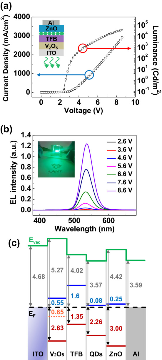
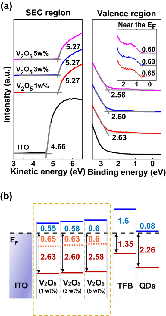
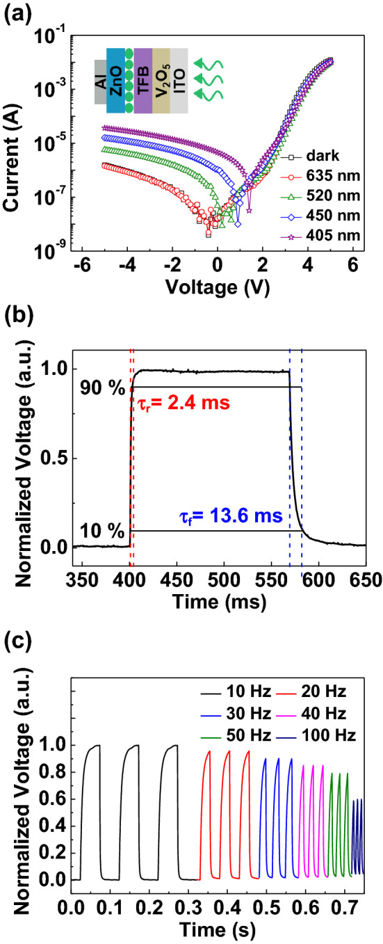
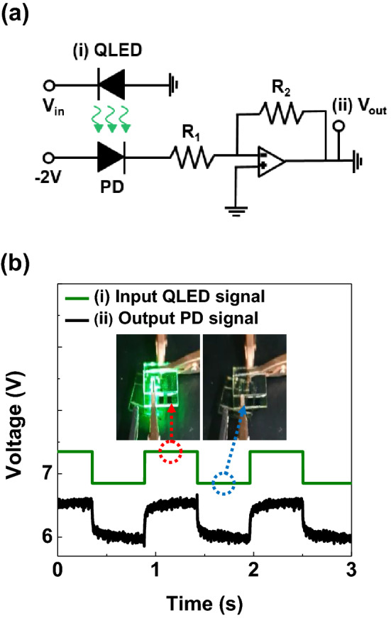
Dual-functional quantum-dots light emitting diodes (QLEDs) have been fabricated using solution processable vanadium oxide (V2O5) hole injection layer to control the carrier transport behavior. The device shows selectable functionalities of photo-detecting and light-emitting behaviors according to the different operating voltage conditions. The device emitted a bright green light at the wavelength of 536 nm, and with the maximum luminance of 31,668 cd/m2 in a forward bias of 8.6 V. Meanwhile, the device could operate as a photodetector in a reverse bias condition. The device was perfectly turned off in a reverse bias, while an increase of photocurrent was observed during the illumination of 520 nm wavelength light on the device. The interfacial electronic structure of the device prepared with different concentration V2O5 solution was measured in detail using x-ray and ultraviolet photoelectron spectroscopy. Both the highest occupied molecular orbital and the gap state levels were moved closer to the Fermi level, according to increase the concentration of V2O5 solution. The change of gap state position enables to fabricate a dual-functional QLEDs. Therefore, the device could operate both as a photodetector and as a light-emitting diode with different applied bias. The result suggests that QLEDs can be used as a photosensor and as a light-emitting diode for the future display industry.
Conflict of interest statement
The authors declare no competing interests.
Figures


References
-
- Zanella A, Bui N, Castellani A, Vangelista L, Zorzi M. Internet of things for smart cities. IEEE Internet Things J. 2014;1:22–32. doi: 10.1109/JIOT.2014.2306328. - DOI
-
- Ortiz AM, Hussein D, Park S, Han SN, Crespi N. The cluster between internet of things and social networks: review and research challenges. IEEE Internet Things J. 2014;1:206–215. doi: 10.1109/JIOT.2014.2318835. - DOI
-
- Lutai, L., Kharchenko, V., Fedorenko, R. & Fedorenko, M. Expert assessment of post accidence monitoring systems with multi-version structures. In 2018 IEEE 9th International Conference on Dependable Systems, Services and Technologies (DESSERT) (2018).
-
- Leng T, et al. Printed graphene/WS2 battery-free wireless photosensor on papers. 2D Mater. 2020;7:024004. doi: 10.1088/2053-1583/ab602f. - DOI
-
- Liao, T. S., Lin, H. N. & Lee, L. J. Simplified and universal resistance response of gas sensor of IoT circuit platform. In 2019 IEEE International Instrumentation and Measurement Technology Conference (I2MTC) (2019).
Grants and funding
LinkOut - more resources
Full Text Sources
Other Literature Sources
Miscellaneous
