. 2021 Mar:222:113198.
doi: 10.1016/j.ultramic.2020.113198. Epub 2020 Dec 30.

Differential electron yield imaging with STXM

Affiliations

Differential electron yield imaging with STXM

William A Hubbard et al. Ultramicroscopy. 2021 Mar.

Abstract

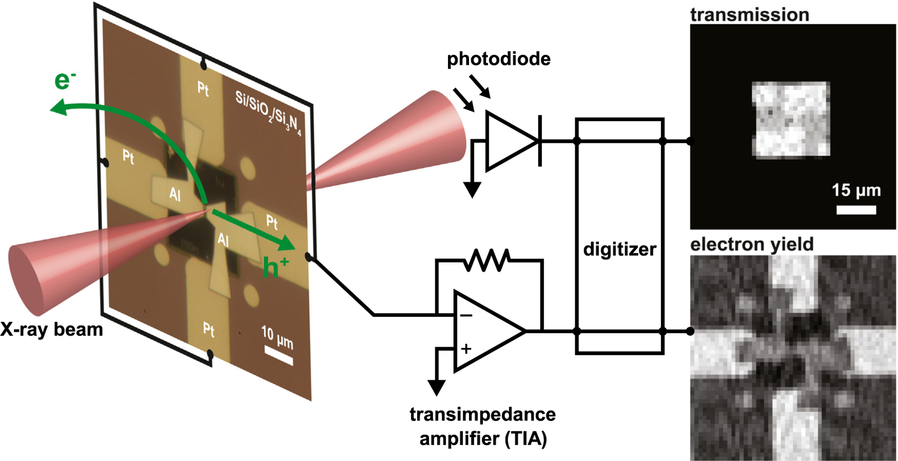
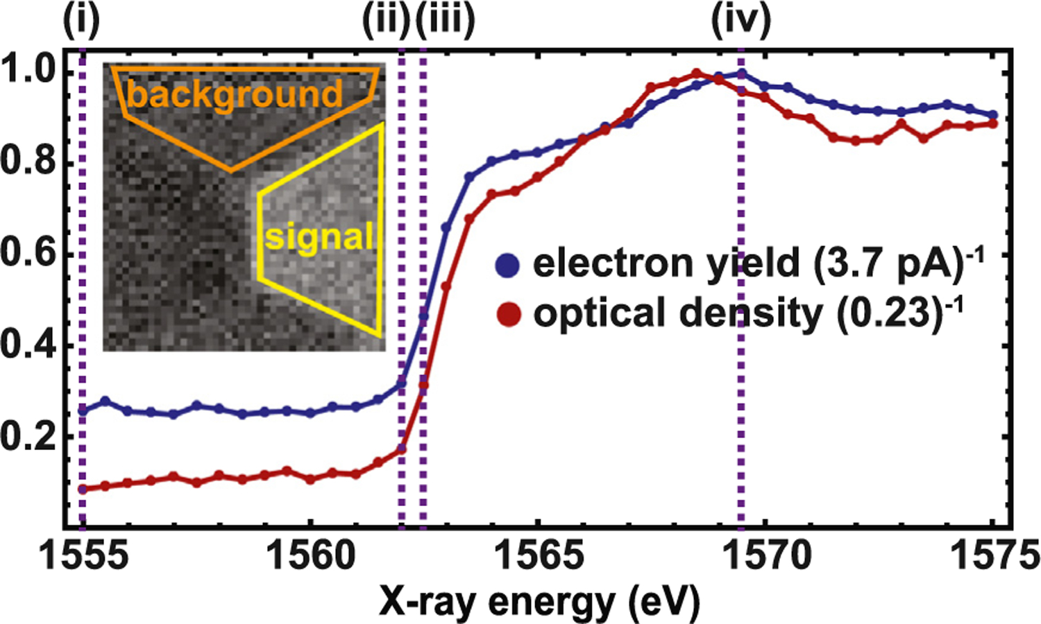
Total electron yield (TEY) imaging is an established scanning transmission X-ray microscopy (STXM) technique that gives varying contrast based on a sample's geometry, elemental composition, and electrical conductivity. However, the TEY-STXM signal is determined solely by the electrons that the beam ejects from the sample. A related technique, X-ray beam-induced current (XBIC) imaging, is sensitive to electrons and holes independently, but requires electric fields in the sample. Here we report that multi-electrode devices can be wired to produce differential electron yield (DEY) contrast, which is also independently sensitive to electrons and holes, but does not require an electric field. Depending on whether the region illuminated by the focused STXM beam is better connected to one electrode or another, the DEY-STXM contrast changes sign. DEY-STXM images thus provide a vivid map of a device's connectivity landscape, which can be key to understanding device function and failure. To demonstrate an application in the area of failure analysis, we image a 100 nm, lithographically-defined aluminum nanowire that has failed after being stressed with a large current density.

Keywords: Electron yield; Failure analysis; STXM; Scanning transmission X-ray microscopy; TEY; XBIC.


Conflict of interest statement

Declaration of competing interest

The authors declare that they have no known competing financial interests or personal relationships that could have appeared to influence the work reported in this paper.

Figures

Fig. 1.
Fig. 1.
Experiment overview. The sample (optical image on left) consists of a 200 μm-thick silicon chip supporting a 20 nm-thick silicon nitride membrane. Platinum leads over the silicon contact an aluminum pattern that tapers to an unresolved wire in the membrane’s center. Here all of the Pt leads are shorted together to produce a TEY image. As the X-ray beam (red) scans the sample, the signal from the photodiode and the transimpedance amplifier (i.e. TIA, or current meter) are digitized simultaneously to form the images on the right. The photodiode signal generates the standard STXM image (top right). The TIA measures the current produced in the sample by the X-ray beam (bottom right). When the beam ejects electrons from the sample, the resulting hole current is positive and is displayed with bright contrast.
Fig. 2.
Fig. 2.
STXM and DEY imaging of the Al nanowire device. These images of the device of Fig. 1 are acquired with the left electrode grounded and the right electrode attached to the TIA (indicated schematically here with an ‘‘I’’ circumscribed by a circle). The field of view in these images lies within the X-ray transparent center of Fig. 1 images, where the photodiode signal is bright. The standard STXM image (left) shows both Al leads with the same contrast, while the DEY image (right) indicates that only the Al lead on the right is electrically connected to the TIA. The red box indicates the region shown in Fig. 3.
Fig. 3.
Fig. 3.
Ptychography and DEY imaging of the Al nanowire device. Retracting the photodiode and scanning over the region outlined in red in Fig. 2 produces, after reconstruction, a ptychography image (top) that reveals the break in the Al nanowire. The simultaneously acquired electron yield image (bottom) has the inferior resolution, relative to ptychography, of standard STXM, but it nonetheless reveals a surprising feature: electrical connectivity spans the ‘break’ in the Al wire that is seen in ptychographic image.
Fig. 4.
Fig. 4.
STEM imaging of the Al nanowire device. The Al wire of Figs. 1–3 is imaged with standard STEM (BF, ADF, and HAADF), STEM EDS elemental mapping (Al and O), and STEM SEEBIC. The BF and SEEBIC images are the electron microscopy analogues of the previously-shown STXM (Fig. 2) and DEY images (Figs. 2–3), respectively. The STEM images show similar contrast but significantly better spatial resolution relative to their analogous X-ray images.
Fig. 5.
Fig. 5.
STXM and electron yield images at four representative X-ray beam energies. The beam energy for each column of representative images (see Fig. 6) is indicated. The electrodes are almost invisible in the raw photodiode (upper row) and calculated optical density (middle row) images below 1562 eV, while they are easily seen in the electron yield images (bottom row) over the entire energy range scanned (1555–1575 eV). The electron yield images are acquired with the circuit as indicated in Figs. 2–3. The contrast scale is held fixed for each row of images.
Fig. 6.
Fig. 6.
Electron yield and optical density of an Al electrode as a function of incident beam energy. Signal on the right electrode (inset, yellow) is plotted for the electron yield (blue curve) and optical density (red curve). Electron yield is measured relative to the background reference region (inset, orange). Both plots are normalized by dividing by the maximum value measured for each, which is indicated in the plot legend. Dashed lines indicate images shown in Fig. 5.

References

    1. Behyan S, Haines B, Karanukaran C, Wang J, Obst M, Tyliszczak T, Urquhart SG, Surface detection in a STXM microscope, AIP Conf. Proc 1365 (1) (2011) 184–187, 10.1063/1.3625335. - DOI
    1. Vila-Comamala J, Jefimovs K, Raabe J, Pilvi T, Fink RH, Senoner M, Maaßdorf A, Ritala M, David C, Advanced thin film technology for ultrahigh resolution X-ray microscopy, Ultramicroscopy 109 (11) (2009) 1360–1364, http://dx.doi.org/10.1016/j.ultramic.2009.07.005 , URL http://dx.doi.org/10.1016/j.ultramic.2009.07.005http://www.sciencedirect.com/science/article/pii/S0304399109001661, URL http://www.sciencedirect.com/science/article/pii/S0304399109001661 . - DOI - PubMed
    1. Obst M, Schmid G, 3D chemical mapping: Application of scanning transmission (soft) X-ray microscopy (STXM) in combination with angle-scan tomography in bio-, geo-, and environmental sciences, Methods Mol. Biol 1117 (2014) 757–781, 10.1007/978-1-62703-776-1_34. - DOI - PubMed
    1. Rightor EG, Hitchcock AP, Ade H, Leapman RD, Urquhart SG, Smith AP, Mitchell G, Fischer D, Shin HJ, Warwick T, Spectromicroscopy of poly(ethylene terephthalate): Comparison of spectra and radiation damage rates in X-ray absorption and electron energy loss, J. Phys. Chem. B 101 (11) (1997) 1950–1960, 10.1021/jp9622748. - DOI
    1. Leontowich AFG, Hitchcock AP, Egerton RF, Radiation damage yields across the carbon 1s excitation edge, J. Electron Spectrosc. Relat. Phenom 206 (2016) 58–64, http://dx.doi.org/10.1016/j.elspec.2015.11.010 , URL http://dx.doi.org/10.1016/j.elspec.2015.11.010http://www.sciencedirect.com/science/article/pii/S0368204815002844, URL http://www.sciencedirect.com/science/article/pii/S0368204815002844 . - DOI