. 2021 Jan 22;12(1):543.
doi: 10.1038/s41467-020-20721-z.

Tunnel field-effect transistors for sensitive terahertz detection

Affiliations

Tunnel field-effect transistors for sensitive terahertz detection

I Gayduchenko et al. Nat Commun. .

Abstract

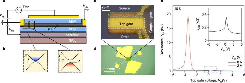
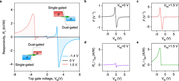
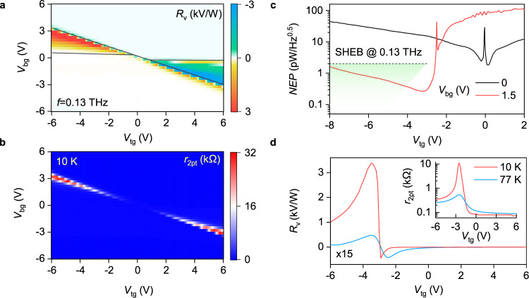
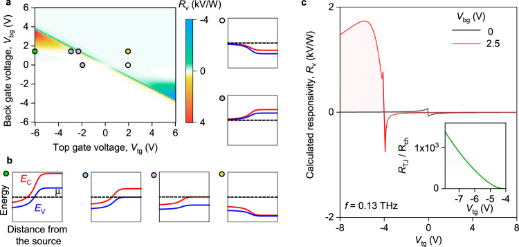
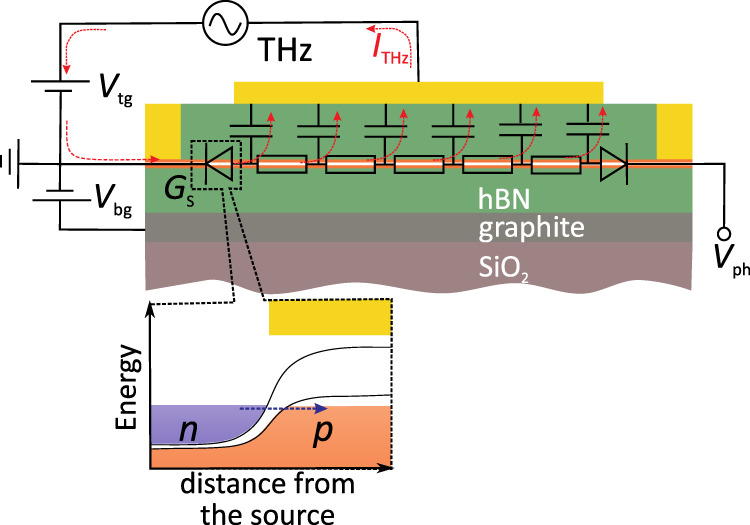
The rectification of electromagnetic waves to direct currents is a crucial process for energy harvesting, beyond-5G wireless communications, ultra-fast science, and observational astronomy. As the radiation frequency is raised to the sub-terahertz (THz) domain, ac-to-dc conversion by conventional electronics becomes challenging and requires alternative rectification protocols. Here, we address this challenge by tunnel field-effect transistors made of bilayer graphene (BLG). Taking advantage of BLG's electrically tunable band structure, we create a lateral tunnel junction and couple it to an antenna exposed to THz radiation. The incoming radiation is then down-converted by the tunnel junction nonlinearity, resulting in high responsivity (>4 kV/W) and low-noise (0.2 pW/[Formula: see text]) detection. We demonstrate how switching from intraband Ohmic to interband tunneling regime can raise detectors' responsivity by few orders of magnitude, in agreement with the developed theory. Our work demonstrates a potential application of tunnel transistors for THz detection and reveals BLG as a promising platform therefor.


Conflict of interest statement

The authors declare no competing interests.

Figures

Fig. 1
Fig. 1. Dual-gated bilayer graphene THz detector.
a Schematic of an hBN encapsulated dual-gated BLG transistor. THz radiation is incident on a broadband antenna connected to the source (S) and gate terminals yielding modulation of the top gate-to-source voltage (Vtg) while the back gate voltage (Vbg) is fixed. The build-up photovoltage Vph is read out between the source and drain (D) terminals. b Band structure of the BLG at the interface between the n-doped bottom gate-sensitive region and dual-gated p-doped channel (Δ is the induced band gap). Blue and red colours illustrate conduction and valence bands fillings, respectively. Note, even for a single-gated region, a finite band gap appears in the energy dispersion due to the difference in on-site energies between the top and bottom graphene layers. c, d Optical photographs of the fabricated dual-gated detector. The source and top-gate terminals are connected to a broadband bow-tie antenna. e The two-terminal resistance of our BLG device, r2pt, as a function of Vtg for two representative Vbg = 0 and Vbg = 2 V. Inset: Zoomed-in r2pt(Vtg) for Vbg = 0 V. T = 10 K.
Fig. 2
Fig. 2. Tunnelling-assisted THz detection.
a Detector responsivity, Rv, as a function of Vtg for Vbg = 0 V (black), Vbg = −1.4 V (blue) and Vbg = 1.5 V (red) measured in response to f = 0.13 THz radiation. T = 10 K. Inset illustrates band profiles in the vicinity of the single and dual-gated interface when Vbg and Vtg are of opposite polarities. Green arrows illustrate interband tunnelling. b, c Normalized transconductance F versus Vtg obtained by numerical differentiation of the device resistance for Vbg = 0 V (b) and Vbg = 1.5 V (c). Note, F(Vtg) dependencies are fairly symmetric whereas the Rv(Vtg) is highly asymmetric for the same Vbg (a). d, e Rv from a normalized to the channel resistance r2pt as a function of Vtg for given Vbg.
Fig. 3
Fig. 3. Performance of the BLG TFET detector.
a Responsivity of our detector as a function of Vbg and Vtg recorded in response to f = 0.13 THz radiation. The black lines demark the (Vtg, Vtg) regions where the tunnel junction configuration is realized. b r2pt(Vtg, Vtg) map measured at T = 10 K. The appearance of highly resistive regions (red) points out to the band gap opening in BLG. c NEP of our detector at given Vbg determined using the Johnson–Nyquist relation for the noise spectral density. Horizontal line marks NEP level for SHEBs operating at the same f and T = 4.2 K (see Supplementary Note 3 for a detailed comparison of the BLG-TFET with other THz detectors). Green shaded region indicates the spread in NEP for SHEBs at higher f. d Temperature dependence of Rv(Vtg) and r2pt(Vtg) (inset) at Vbg = 1.5 V.
Fig. 4
Fig. 4. Modelling tunnelling-assisted THz detection.
a Calculated Rv(Vtg, Vbg) map of our dual-gated BLG device in response to f = 0.13 THz radiation. b Calculated band profiles for different (Vtg, Vbg) configurations indicated by the coloured symbols in a. White, grey, yellow, and pink symbols point to the band diagrams of the FET mode whereas the green and blue symbols correspond to the regime of interband tunnelling. Red, blue, and black lines illustrate conduction band minimum (EC), valence band maximum (EV), and the chemical potential (μ), respectively. c Line cuts of the map in (a) for Vbg = 0 V and Vbg = 2.5 V. The radiation resistance of the antenna Zrad ≈ 75 Ω was used for these calculations (“Methods”). Inset: The ratio between the tunnel junction, RTJ, contribution to the responsivity and that of the channel nonlinearity, Rch, for Vbg = 2.5 V.
Fig. 5
Fig. 5. Equivalent circuit of the BLG-TFET detector.
Antenna is modelled as an equivalent voltage source Vant that generates ac current ITHz (red arrows) flowing into the source and escaping the FET channel through the gate capacitance. Rectification occurs mainly at the tunnel barrier between source and channel (see band alignment profile in the inset) with voltage-dependent conductance GS. The doping level and the band gap size is controlled via a simultaneous action of the top and bottom gate voltages, Vtg and Vtg, respectively. The photovoltage, Vph, is read out between the source and drain terminals.

References

    1. Dyakonov M, Shur M. Detection, mixing, and frequency multiplication of terahertz radiation by two-dimensional electronic fluid. IEEE Trans. Electron. Dev. 1996;43:380–387. doi: 10.1109/16.485650. - DOI
    1. Knap W, et al. Field effect transistors for terahertz detection: physics and first imaging applications. J. Infrared Millimeter Terahertz Waves. 2009;30:1319–1337.
    1. Boppel S, et al. CMOS integrated antenna-coupled field-effect transistors for the detection of radiation from 0.2 to 4.3 THz. IEEE Trans. Microwave Theory Tech. 2012;60:3834–3843. doi: 10.1109/TMTT.2012.2221732. - DOI
    1. Hou H, Liu Z, Teng J, Palacios T, Chua S. High temperature terahertz detectors realized by a GaN high electron mobility transistor. Sci. Rep. 2017;7:46664. doi: 10.1038/srep46664. - DOI - PMC - PubMed
    1. Viti L. Thermoelectric graphene photodetectors with sub-nanosecond response times at terahertz frequencies. Nanophotonics. 2020;10:89–98. doi: 10.1515/nanoph-2020-0255. - DOI