. 2021 Jan 27;11(1):2304.
doi: 10.1038/s41598-021-81712-8.

Atomic scale displacements detected by optical image cross-correlation analysis and 3D printed marker arrays

Affiliations

Atomic scale displacements detected by optical image cross-correlation analysis and 3D printed marker arrays

Tobias Frenzel et al. Sci Rep. .

Abstract

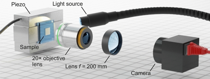
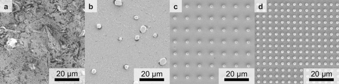
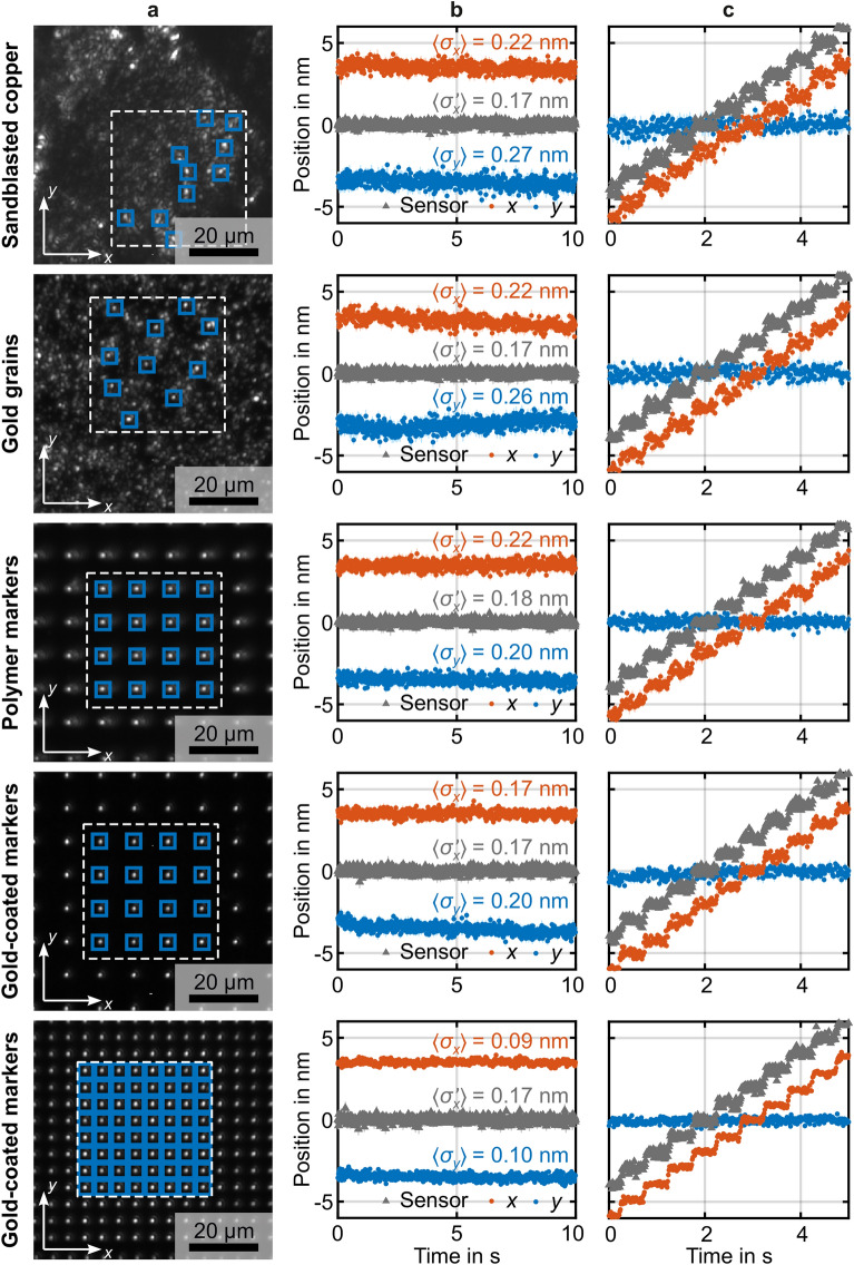
For analyzing displacement-vector fields in mechanics, for example to characterize the properties of 3D printed mechanical metamaterials, routine high-precision position measurements are indispensable. For this purpose, nanometer-scale localization errors have been achieved by wide-field optical-image cross-correlation analysis. Here, we bring this approach to atomic-scale accuracy by combining it with well-defined 3D printed marker arrays. By using an air-lens with a numerical aperture of [Formula: see text] and a free working distance of [Formula: see text], and an [Formula: see text] array of markers with a diameter of [Formula: see text] and a period of [Formula: see text], we obtain 2D localization errors as small as [Formula: see text] in [Formula: see text] measurement time ([Formula: see text]). The underlying experimental setup is simple, reliable, and inexpensive, and the marker arrays can easily be integrated onto and into complex architectures during their 3D printing process.


Conflict of interest statement

The authors declare no competing interests.

Figures

Figure 1
Figure 1
Scheme of the simple optical setup used to determine two-dimensional displacement vectors of a macroscopic sample with atomic-scale localization errors. The surface of a sample is illuminated by unpolarized visible white light from a filtered incandescent source impinging onto the sample under an angle. An objective lens (with focal length f=8.25mm) together with a tube lens (with focal length f=200mm) images the sample surface onto a digital black/white camera. The objective lens has a numerical aperture of NA=0.4 and a free working distance of 11.2mm. The images acquired by the camera are processed using image cross-correlation analysis. We can displace the sample in the plane normal to the optical axis by a precision piezoelectric stage. The setup is located on a vibration-isolated optical table and enclosed in a box to reduce vibrations and drifts between the sample and the camera position.
Figure 2
Figure 2
Top-view electron micrographs of four of the five investigated samples. (a) Sample #1 is a sandblasted copper surface. (b) Sample #2 is a glass substrate with randomly distributed micrometer-sized gold grains on top. Sample #3 (not depicted) is a glass substrate with a square array of polymer markers with period a=10μm on top, fabricated by 3D laser printing. Without metal coating, this sample cannot easily be imaged by electron microscopy. (c) Sample #4 is as sample #3, but coated with a 54nm thin film of gold. (d) Sample #5 is as sample #4, but with a period of a=5μm.
Figure 3
Figure 3
Summary of data obtained from five different samples #1 to #5 (cf. Fig. 2). Column (a) exhibits an example optical image with the used regions of interest (ROI) indicated by the blue squares. Each ROI comprises 30×30 camera pixels. The ROI lie in a footprint of 40μm2 indicated by the dashed white square. Column (b) shows results obtained from the optical-image cross-correlation approach for the x-component (red) and the y-component (blue). For comparison, the read-out signal from the capacitive sensor of the piezoelectric actuator is shown in gray. This signal has been shifted vertically for clarity. For each of the 800 data points, we obtain localization errors σx and σy. The mean values σx and σx over 800 measurements are indicated. σx is the corresponding value for the capacitive sensor, for the same measurement time of 12.5ms. In column (b), the piezoelectric actuator has not been moved intentionally. In contrast, in column (c), the piezoelectric actuator has been moved in a staircase manner with 1nm high steps each 0.5s.

Similar articles

Cited by

References

    1. Griffiths DJ. Introduction to Quantum Mechanics. Cambridge: Cambridge University Press; 2017.
    1. Knuuttila JV, Tikka PT, Salomaa MM. Michelson interferometer for imaging surface acoustic wave fields. Opt. Lett. 2000;25:613–615. doi: 10.1364/OL.25.000613. - DOI - PubMed
    1. Wehner MU, Ulm MH, Wegener M. Scanning interferometer stabilized by use of Pancharatnam's phase. Opt. Lett. 1997;22:1455–1457. doi: 10.1364/OL.22.001455. - DOI - PubMed
    1. Feldmann M, editor. Nanolithography: The Art of Fabricating Nanoelectronic and Nanophotonic Devices and Systems. Sawston: Woodhead Publ. Ltd.; 2014.
    1. Gieseler J, Deutsch B, Quidant R, Novotny L. Subkelvin parametric feedback cooling of a laser-trapped nanoparticle. Phys. Rev. Lett. 2012;109:103603. doi: 10.1103/PhysRevLett.109.103603. - DOI - PubMed

LinkOut - more resources