Review
. 2020 Dec 6;8(2):2002488.
doi: 10.1002/advs.202002488. eCollection 2021 Jan.

van der Waals Magnets: Material Family, Detection and Modulation of Magnetism, and Perspective in Spintronics

Affiliations
Review

van der Waals Magnets: Material Family, Detection and Modulation of Magnetism, and Perspective in Spintronics

Shengxue Yang et al. Adv Sci (Weinh). .

Abstract

van der Waals (vdW) materials exhibit great potential in spintronics, arising from their excellent spin transportation, large spin-orbit coupling, and high-quality interfaces. The recent discovery of intrinsic vdW antiferromagnets and ferromagnets has laid the foundation for the construction of all-vdW spintronic devices, and enables the study of low-dimensional magnetism, which is of both technical and scientific significance. In this review, several representative families of vdW magnets are introduced, followed by a comprehensive summary of the methods utilized in reading out the magnetic states of vdW magnets. Thereafter, it is shown that various electrical, mechanical, and chemical approaches are employed to modulate the magnetism of vdW magnets. Finally, the perspective of vdW magnets in spintronics is discussed and an outlook of future development direction in this field is also proposed.

Keywords: detection methods; material families; modulation methods; spintronics; van der Waals magnets.


Conflict of interest statement

The authors declare no conflict of interest.

Figures

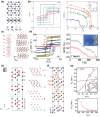
Figure 1
Figure 1
Basic properties of transition metal halides. a) The crystallographic structures of monolayer transition metal dihalides (left panel) and trihalides (right panel). Reproduced with permission.[ 111 ] Copyright 2019, Springer Nature. b) The phase diagram of Cr trihalides versus temperature and magnetic field. Reproduced with permission.[ 33 ] Copyright 2019, American Chemical Society. c) Two possible stacking orders of Cr trihalides. Reproduced with permission.[ 24 ] Copyright 2019, Springer Nature. d) The possible spatial distribution of magnetic order and stacking order in bulk CrI3 from the surface layer to the inner layer. Reproduced with permission.[ 35 ] Copyright 2020, American Chemical Society. e) The calculated spin‐resolved band structures of Fe dihalides. Reproduced with permission.[ 42 ] Copyright 2017, American Chemical Society.
Figure 2
Figure 2
Basic properties of transition‐metal phosphorous tri‐chalcogenides and the isostructural Cr(Si/Ge)Te3. a) The crystal structure of these isostructural compounds. Reproduced with permission.[ 111 ] Copyright 2019, Springer Nature. b) The temperature dependence of peak positions for P 2 mode in MnPS3 with different thicknesses. Reproduced with permission.[ 58 ] Copyright 2019, American Chemical Society. c) The temperature dependence of peak intensities for the magnetic‐order induced P 1a mode in FePS3 with different thicknesses. Reproduced with permission.[ 55 ] Copyright 2016, American Chemical Society. d) The temperature dependence of peak splitting for P 2 mode in NiPS3 with different thicknesses. Reproduced with permission.[ 56 ] Copyright 2019, Springer Nature. e) The schematic diagram of Neel‐type and zigzag‐type magnetic structures for MPQ3. Reproduced with permission.[ 60 ] Copyright 2015, American Physical Society. f) Optical micrograph of few‐layer CrGeTe3 and the respective characterization of magnetism using MOKE at different temperatures. Scale bar: 10 µm. g) The T C of CrGeTe3 versus number of layers. Reproduced with permission.[ 12 ] Copyright 2017, Springer Nature.
Figure 3
Figure 3
Basic properties of ternary iron‐based tellurides. a) The crystal structure of Fe3GeTe2. Reproduced with permission.[ 21 ] Copyright 2018, Springer Nature. b) The magnetism characterization of Fe3GeTe2. The left panel: the field‐dependent Rxy measured on a 12 nm thick sample at different temperatures. The right panel: temperature‐dependent MCD measurements of Fe3GeTe2 with different thicknesses (dots) and the corresponding fitting results using critical power law (lines). The inset shows the derived critical exponent β as a function of thickness. Reproduced with permission.[ 76 ] Copyright 2018, Springer Nature. c) The crystal structure of Fe4GeTe2. d) The magnetism characterization of Fe4GeTe2. The left panel: the anomalous Hall conductivity versus sweeping magnetic fields for an 11‐layer sample under different temperatures. The right panel: temperature‐dependent MCD measurements on a 7‐layer sample with (black circles)/without (red circles) a 0.5 T out‐of‐plane field, while the inset displays the optical micrograph of the seven‐layer sample and the circular polarization configuration for MCD measurements. Reproduced with permission.[ 81 ] Copyright 2020, American Association for the Advancement of Science. e,f) Two existing crystal structures of Fe5GeTe2. Reproduced with permission.[ 84 ] Copyright 2018, Wiley‐VCH. g) The magnetism characterization of a 28 nm thick Fe5GeTe2 sample. Top panel: the hysteresis loop measured using AHE at 270 K with external magnetic field vertical/parallel to the basal plane of sample, and the inset is a magnification at around zero field. Bottom panel: the temperature dependence of remnant Hall resistance at a temperature range of 200–280 K. Reproduced with permission.[ 83 ] Copyright 2019, American Chemical Society.
Figure 4
Figure 4
Basic properties of transition metal oxyhalides and transition metal dichalcogenides. a) The crystal structure of transition metal oxyhalides. b) Temperature dependence of the peak position for A g 2 mode in CrOCl (black dots), and the anharmonic fitting results (red line). Reproduced with permission.[ 93 ] Copyright 2019, American Chemical Society. c) The temperature‐dependent magnetic susceptibility measured on chemically exfoliated FeOCl nanoflakes using the field‐cooling mode (blue, magnetic field: 1T) and zero‐field‐cooling mode (orange), and the inset shows the field‐dependent magnetization measured at 2 and 300 K. Reproduced with permission.[ 96 ] Copyright 2020, American Chemical Society. d) The calculated spin‐splitting (left, where red and black denotes the majority and minority spins, respectively), nonmagnetic (middle), and the experimentally observed (right) electronic structures of monolayer VSe2. Reproduced with permission.[ 101 ] Copyright 2018, American Chemical Society. e) The atomic‐resolution scanning tunneling microscopy image of monolayer VSe2 grown on MoS2 substrate. Reproduced with permission.[ 102 ] Copyright 2019, American Chemical Society. f) The elemental‐resolved hysteresis loops of Co (blue) and V (yellow) measured on the MBE‐grown monolayer VSe2 capped by a Co layer using XMCD at 65 K. Reproduced with permission.[ 105 ] Copyright 2019, American Chemical Society. g) The elemental‐resolved XMCD signal of Fe (red) and V (green) as a function of magnetic field measured on the MBE‐grown monolayer VSe2 capped by a Fe layer measured at 300 K. Reproduced with permission.[ 106 ] Copyright 2019, American Physical Society. h) Schematic diagram of spin frustration in VSe2. Reproduced with permission.[ 107 ] Copyright 2019, Wiley‐VCH. i) The measured hysteresis loop of monolayer MnSe2 grown on GaSe substrate at 300 K, and the inset shows the raw data without the subtraction of diamagnetic background. Reproduced with permission.[ 100 ] Copyright 2018, American Chemical Society.
Figure 5
Figure 5
The magnetic transition temperature of the materials mentioned in this work. The bar means that the transition temperature of this material is different for different forms (e.g., the bulk and few‐layer samples). sP: Spin‐Peierls phase, IC: incommensurate phase, PM: paramagnetic phase. The blue dashed line denotes the liquid nitrogen temperature. For details, please refer to the corresponding part in this review.
Figure 6
Figure 6
Detection of magnetism using MOKE, MCD, and PL. a) Direct observation of ferromagnetism in monolayer CrI3 using MOKE and the evolution of magnetic domain structures with sweeping the fields. Reproduced with permission.[ 20 ] Copyright 2017, Nature Publishing Group. b) Direct observation of ferromagnetism in monolayer Fe3GeTe2 using MCD. Reproduced with permission.[ 76 ] Copyright 2018, Springer Nature. c) The PL intensities of right circularly polarized light (red) and left circularly polarized light (blue) in monolayer CrI3 with the magnetic moments aligned downward (left panel) and upward (right panel), while the incident light is always linearly polarized. d) The field‐dependent circular polarization of collected lights in a monolayer CrI3. e) The circular polarization of collected lights versus sweeping the magnetic fields in a bilayer CrI3. Reproduced with permission.[ 113 ] Copyright 2017, Springer Nature. f) The field‐dependent proximity‐induced valley splitting in a CrI3/WSe2 heterostructure. Reproduced with permission.[ 114 ] Copyright 2017, American Association for the Advancement of Science. g) The field‐dependent relative polarization of collected luminescence of monolayer CrBr3 under various polarization configurations for excitation and collection lights, where σ + denotes right circularly polarized light and σ is left circularly polarized light. Reproduced with permission.[ 16 ] Copyright 2019, American Chemical Society.
Figure 7
Figure 7
Detection of magnetism using Raman spectra. a) The temperature‐dependent phonon frequencies of A 1g mode in Fe3GeTe2 (black dots), and the corresponding fitting results using the anharmonic model (the red line). Reproduced with permission.[ 117 ] Copyright 2019, Wiley‐VCH. b) The polar plots of A 1g mode in monolayer CrI3 at 60 K (left panel) and 15 K (right panel) with moments aligned upward (red) and downward (blue). The green arrow represents the polarization of incident light. c) The circular‐polarization resolved Raman measurements for monolayer CrI3 at 60 K (left panel) and 15 K (right panel) with moments aligned upward. σ +/σ means that the excitation and collection are right and left circularly polarized light, respectively. d) The temperature‐dependent Raman measurements on bilayer CrI3 under XY (left panel) and XX configurations (right panel). Reproduced with permission.[ 15 ] Copyright 2019, Springer Nature. e) The field‐dependent Raman measurements on bilayer CrI3 under XX (left panel) and XY configurations (right panel). f) The Raman spectra of bilayer CrI3 at 0 T, −1 T, and 1 T measured under XY configuration. Reproduced with permission.[ 118 ] Copyright 2020, American Chemical Society.
Figure 8
Figure 8
Detection of magnetism using SHG and SSSM. a) Schematic diagram of the lack of inversion center in bilayer CrI3 at the AFM state. Reproduced with permission.[ 15 ] Copyright 2019, Springer Nature. b) The SHG intensity mapping of bilayer CrI3 (marked by the green dot) at 50 K (left panel) and 5 K (right panel). c) The circular‐polarization‐resolved SHG measurements on bilayer CrI3. d) The polar plots of SHG intensities measured on bilayer CrI3 using 900, 970, and 1040 nm incident laser under XX (black dots) and XY (red dots) configurations. The black line and red line are the respective fitting results using nonlinear tensors based on the monoclinic stacked structure. Reproduced with permission.[ 17 ] Copyright 2019, Springer Nature. e) The illustration for the lack of inversion center in MnPS3 at the magnetic ordered state compared with FePS3 and NiPS3. f) The temperature‐dependent SHG intensity along the anticlockwise 60° direction relative to the horizontal axis in the polar plots of bulk MnPS3, FePS3, and NiPS3, and the solid line is the best fitting results using critical power law for MnPS3. Inset shows the polar plots of these three compounds at various temperatures. g) Temperature‐dependent SHG measurements on MnPS3 with different thicknesses. Reproduced with permission.[ 57 ] Copyright 2020, American Physical Society. h) The schematic figure of the SSSM measurements. The gray arrow denotes the single spin in the diamond nitrogen‐vacancy, Z NV denotes the distance between the tip and the surface, and θ NVdenotes the angle of the direction of the single spin and the moments in the sample. i) The measured magnetization map of a CrI3 sample under the transition temperature using SSSM, where 1 and 2 denote bilayer and tri‐layer parts in this CrI3 sample, respectively. j) The line‐cut results of sample magnetic field across the edge of a nine‐layer CrI3 sample before (red line) and after puncture (blue line). Reproduced with permission.[ 19 ] Copyright 2019, American Association for the Advancement of Science.
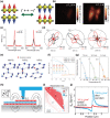
Figure 9
Figure 9
Electrical detection based on TMR. a) The schematic of an MTJ device constructed using Fe3GeTe2, where L1 and L2 represent Fe3GeTe2 flakes with different thickness. b) The measured tunneling resistance of device shown in (a) as a function of magnetic field at 4.2 K. c) The spin polarization for carriers in Fe3GeTe2 versus temperature (black) derived from the TMR measurement results, and the temperature‐dependent anomalous Hall conductivity (red dots) for Fe3GeTe2 derived from the AHE‐based measurements. The red line is the fitting results using power law. Reproduced with permission.[ 124 ] Copyright 2018, American Chemical Society. d) The schematic of an MTJ device based on bilayer CrCl3. Reproduced with permission.[ 125 ] Copyright 2019, American Chemical Society. e) The tunneling current of bilayer CrI3 measured under sweeping the out‐of‐plane fields. f) The tunneling current of bilayer CrI3 as a function of in‐plane fields. Reproduced with permission.[ 22 ] Copyright 2018, American Association for the Advancement of Science. g) The tunneling current of bilayer CrCl3 versus out‐of‐plane and in‐plane fields. Reproduced with permission.[ 125 ] Copyright 2019, American Chemical Society. h) The tunneling conductance of bilayer (left panel) and tri‐layer (right panel) CrCl3 measured under in‐plane magnetic fields. i) The field‐dependent dG/dH for bilayer (left panel) and tri‐layer (right panel) CrCl3. Reproduced with permission.[ 126 ] Copyright 2019, Springer Nature. j) The TMR measured on 13‐layer (left panel) and monolayer (right panel) MnPS3 with out‐of‐plane magnetic fields at different temperatures. Reproduced with permission.[ 127 ] Copyright 2020, American Chemical Society. k) The schematic of unique design for the SPSTM measurements. l) The measured differential tunneling conductance of H‐type stacked bilayer CrBr3 versus out‐of‐plane magnetic field using a Cr tip. The black data denotes the upward sweeping direction of magnetic fields, while red data represents downward. m) The field‐dependent differential tunneling conductance of R‐type stacked bilayer CrBr3 measured using a Cr tip (left panel) or a W tip (right panel). Reproduced with permission.[ 18 ] Copyright 2019, American Association for the Advancement of Science.
Figure 10
Figure 10
Electrical detection based on Hall effect. a) Optical micrograph of a Hall bar device made of Fe5GeTe2 to measure AHE; scale bar: 20 µm. b) The measured Rxy of device in (a) versus sweeping the magnetic fields at 220 K. Reproduced with permission.[ 83 ] Copyright 2019, American Chemical Society. c) The layer‐number‐temperature phase diagram of Fe3GeTe2 defined by the MCD and AHE‐based measurements. Reproduced with permission.[ 21 ] Copyright 2018, Springer Nature. d) The false color optical micrograph of a Hall bar device made of CrGeTe3 capped by a Pt layer. The CrGeTe3 and Pt are denoted in green and gray, respectively. e) The anomalous Hall resistivity measured on device in (d) as a function of magnetic field. f) The characterization of Pt/CrGeTe3 heterostructure using MFM under different magnetic fields, corresponding to the points marked in (e). Reproduced with permission.[ 131 ] Copyright 2019, American Chemical Society. g) Optical micrograph of the Hall micro‐magnetometry (scale bar: 2 µm), the measurement circuits and the schematic of the cross section of the device (top right inset). Top left inset: the atomic‐resolution structure analysis of CrBr3 using transmission electron microscope with the blue and yellow circles representing Cr atoms and Br atoms, respectively, and the scale bar is 1 nm. h) The measured hysteresis loop of bilayer CrBr3 using the Hall micro‐magnetometry. The inset shows the micromagnetic simulated domain structures at the marked points in the hysteresis loop. i) The green dots are the temperature dependence of saturation magnetization in monolayer CrBr3 and the solid lines are the fitting results based on different models (blue: XXZ model with Kitaev interactions, black: 2D Ising model, red: the best fitting results using the power law). Reproduced with permission.[ 134 ] Copyright 2019, Springer Nature.
Figure 11
Figure 11
Electrical modulation of magnetism. a) The schematic of a dual‐gated device based on bilayer CrI3. Reproduced with permission.[ 23 ] Copyright 2018, Springer Nature. b) The MCD signal of monolayer CrI3 versus magnetic field under electron (blue), zero (black) and hole doping (red). Reproduced with permission.[ 139 ] Copyright 2018, Springer Nature. c) The variation of magnetization of bilayer CrI3 as a function of electrical field at zero magnetic field (red/black open circles denote that bilayer CrI3 is initialized by cooling below the transition temperature under a magnetic field of 1 T/−1 T, respectively) and an external magnetic field of 1 T (filled circles). Reproduced with permission.[ 120 ] Copyright 2018, Springer Nature. d) The field‐dependent MCD signal of bilayer CrI3 under different doping levels and types (the negative gate voltage will induce hole doping, while the positive gate voltage will induce electron doping). Reproduced with permission.[ 139 ] Copyright 2018, Springer Nature. e) The schematic of a field‐effect transistor made of few‐layer CrGeTe3 by vdW assembly. f) The field‐dependent magnetization of CrGeTe3 under different hole (left panel) and electron (right panel) doping levels measured by MOKE. Reproduced with permission.[ 112 ] Copyright 2018, Springer Nature. g) The schematic of current control of magnetism in Fe3GeTe2 by SOT in the adjacent Pt layer (left panel) and the current switching of magnetization in Fe3GeTe2 under an in‐plane magnetic field of 50 mT characterized by AHE‐based measurements (right panel). The current direction is parallel to the magnetic‐field direction, which is along the x‐axis marked in the left panel. Reproduced with permission.[ 146 ] Copyright 2019, American Association for the Advancement of Science. h) Left panel: the schematic of a Hall bar device made of CrGeTe3 capped by a Ta layer to realize the current control of magnetism. Right panel: the anomalous Hall resistance of CrGeTe3/Ta heterostructure as a function of in‐plane magnetic field under a current of 100 µA (blue) and −100 µA (red). The current direction is parallel to the magnetic‐field direction, which is along the x‐axis marked in the left panel. Reproduced with permission.[ 147 ] Copyright 2020, Wiley‐VCH.
Figure 12
Figure 12
Mechanical modulation of magnetism. a) Schematic diagram of experimental setup to apply pressure on bulk Fe3GeTe2. b) The anomalous Hall resistivity of bulk Fe3GeTe2 as a function of magnetic field under different hydrostatic pressures. Reproduced with permission.[ 149 ] Copyright 2019, American Physical Society. c) The field‐dependent magnetoresistance of bulk CrGeTe3 under different pressures. Reproduced with permission.[ 75 ] Copyright 2018, American Physical Society. d) Schematic of experimental setup to apply pressure on few‐layer CrI3. e) The tunneling current of bilayer CrI3 versus sweeping magnetic fields under different pressures. Reproduced with permission.[ 152 ] Copyright 2019, Springer Nature. f) The polarization dependence of Raman mode at around 107 cm−1 for a five‐layer CrI3 before (top panel) and after (bottom panel) applying pressure. Reproduced with permission.[ 24 ] Copyright 2019, Springer Nature. g) The spin‐flip field and T C of bilayer CrI3 measured under different pressures. Reproduced with permission.[ 152 ] Copyright 2019, Springer Nature. h) The calculated strain‐dependent energy difference between the AFM and FM phases, magnetization, and T C of monolayer NiBr3. Reproduced with permission.[ 156 ] Copyright 2019, Royal Society of Chemistry. i) The calculated temperature‐dependent magnetization of monolayer Cr2Ge2Se6 under different strains. Reproduced with permission.[ 26 ] Copyright 2019, American Physical Society.
Figure 13
Figure 13
Chemical modulation of magnetism. a) The coercivity of Fe3GeTe2 (rectangular) and Fe2.7GeTe2 (circle) with different thicknesses at 10 (blue) and 20 K (red). Reproduced with permission.[ 79 ] Copyright 2019, American Chemical Society. b) The magnetic moment of bulk (Fe1− xCox)3GeTe2 versus out‐of‐plane magnetic fields at different Co contents. Reproduced with permission.[ 80 ] Copyright 2019, American Physical Society. c) The Curie–Weiss temperature and T C of bulk CrCl3− xBrx as a function of Br content. Reproduced with permission.[ 25 ] Copyright 2018, Wiley‐VCH. d) The temperature‐dependent magnetization of CrGeTe3 measured under an external magnetic field of 5000 Oe (red), and the temperature‐dependent magnetization of tetra‐butyl ammonium intercalated CrGeTe3 measured under a magnetic field of 1000 Oe (black). Reproduced with permission.[ 165 ] Copyright 2019, American Chemical Society. e) The atomic force microscopic image (left panel) and optical microscopic image (right panel) of an exfoliated CrCl3− xBrx flake. Reproduced with permission.[ 25 ] Copyright 2018, Wiley‐VCH.
Figure 14
Figure 14
Perspective of vdW magnets in spintronics. a) Schematic diagram of the MTJ using half‐metallic vdW magnets as electrodes. Reproduced with permission.[ 42 ] Copyright 2017, American Chemical Society. b) The schematic of the spin splitting of band structures in monolayer graphene. The red and blue arrows denote different spin directions of carriers. c) The schematic of the nonlocal transport measurements in graphene. The carriers with different spins are distinguished by the color (blue and red). There is no transverse charge current but exists net spin current. d) Left panel: the R nl of monolayer graphene proximitized with CrBr3 as a function of gate voltage at different external magnetic fields. The Dirac point is denoted by the zero point in the abscissa axis. Right panel: the temperature‐dependent R nl,D of pristine graphene (black) and graphene proximitized with CrBr3 (red). The T C of CrBr3 is marked by the red arrow. Reproduced with permission.[ 171 ] Copyright 2020, Wiley‐VCH. e) Field‐dependent nonlocal Hanle spin precession measurements for the graphene proximitized with CrGeTe3 at different temperatures. Reproduced with permission.[ 174 ] Copyright 2019, IOP Publishing Ltd. f) Schematic of voltage torque‐MRAM (left panel) and SOT‐MRAM (right panel) made of magnetic vdW materials. Reproduced with permission.[ 170 ] Copyright 2019, Springer Nature. g) Schematic of spin tunneling field‐effect transistors made of bilayer CrI3. Reproduced with permission.[ 177 ] Copyright 2019, Springer Nature.

References

    1. Yan H., Feng Z., Shang S., Wang X., Hu Z., Wang J., Zhu Z., Wang H., Chen Z., Hua H., Lu W., Wang J., Qin P., Guo H., Zhou X., Leng Z., Liu Z., Jiang C., Coey M., Liu Z., Nat. Nanotechnol. 2019, 14, 131. - PubMed
    1. Vaz C. A. F., Bland J. A. C., Lauhoff G., Rep. Prog. Phys. 2008, 71, 056501.
    1. Mermin N. D., Wagner H., Phys. Rev. Lett. 1966, 17, 1133.
    1. Novoselov K. S., Geim A. K., Morozov S. V., Jiang D., Zhang Y., Dubonos S. V., Grigorieva I. V., Firsov A. A., Science 2004, 306, 666. - PubMed
    1. Bolotin K. I., Sikes K. J., Jiang Z., Klima M., Fudenberg G., Hone J., Kim P., Stormer H. L., Solid State Commun. 2008, 146, 351.

LinkOut - more resources