

Nanopatterning of Weak Links in Superconducting Oxide Interfaces
- PMID: 33557305
- PMCID: PMC7914727
- DOI: 10.3390/nano11020398
Nanopatterning of Weak Links in Superconducting Oxide Interfaces
Abstract
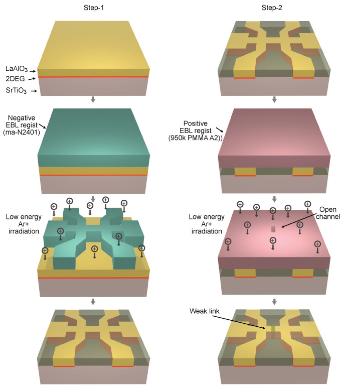
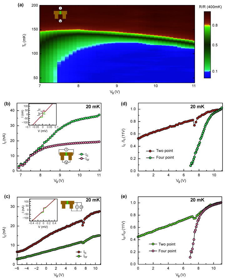
The interface between two wide band-gap insulators, LaAlO3 and SrTiO3 (LAO/STO), hosts a quasi-two-dimensional electron gas (q2DEG), two-dimensional superconductivity, ferromagnetism, and giant Rashba spin-orbit coupling. The co-existence of two-dimensional superconductivity with gate-tunable spin-orbit coupling and multiband occupation is of particular interest for the realization of unconventional superconducting pairing. To investigate the symmetry of the superconducting order parameter, phase sensitive measurements of the Josephson effect are required. We describe an approach for the fabrication of artificial superconducting weak links at the LAO/STO interface using direct high-resolution electron beam lithography and low-energy argon ion beam irradiation. The method does not require lift-off steps or sacrificial layers. Therefore, resolution is only limited by the electron beam lithography and pattern transfer. We have realized superconducting weak links with a barrier thickness of 30-100 nm. The barrier transparency of the weak links can be controlled by the irradiation dose and further tuned by a gate voltage. Our results open up new possibilities for the realization of quantum devices in oxide interfaces.
Keywords: LaAlO3/SrTiO3 interface; nanopatterned materials; top-down lithography; two-dimensional superconductivity.
Conflict of interest statement
The authors declare no conflict of interest.
Figures
Similar articles
-
Effect of electrostatic confinement on the dome-shaped superconducting phase diagram at the LaAlO3/SrTiO3 interface.Sci Rep. 2024 Oct 30;14(1):26177. doi: 10.1038/s41598-024-77460-0. Sci Rep. 2024. PMID: 39478102 Free PMC article.
-
Competition between electron pairing and phase coherence in superconducting interfaces.Nat Commun. 2018 Jan 29;9(1):407. doi: 10.1038/s41467-018-02907-8. Nat Commun. 2018. PMID: 29379023 Free PMC article.
-
Superconductivity with Rashba spin-orbit coupling and magnetic field.J Phys Condens Matter. 2013 Sep 11;25(36):362201. doi: 10.1088/0953-8984/25/36/362201. Epub 2013 Aug 9. J Phys Condens Matter. 2013. PMID: 23934775
-
Controlling unconventional superconductivity in artificially engineeredf-electron Kondo superlattices.J Phys Condens Matter. 2021 May 28;33(27). doi: 10.1088/1361-648X/abfdf2. J Phys Condens Matter. 2021. PMID: 33946054 Review.
-
KTaO3 -The New Kid on the Spintronics Block.Adv Mater. 2022 Mar;34(9):e2106481. doi: 10.1002/adma.202106481. Epub 2022 Jan 18. Adv Mater. 2022. PMID: 34961972 Review.
Cited by
-
Superconducting Properties and Electron Scattering Mechanisms in a Nb Film with a Single Weak-Link Excavated by Focused Ion Beam.Materials (Basel). 2021 Nov 28;14(23):7274. doi: 10.3390/ma14237274. Materials (Basel). 2021. PMID: 34885429 Free PMC article.
References
LinkOut - more resources
Full Text Sources
Other Literature Sources
Miscellaneous
