. 2021 Feb 26;12(1):1299.
doi: 10.1038/s41467-021-21565-x.

Electromechanically reconfigurable optical nano-kirigami

Affiliations

Electromechanically reconfigurable optical nano-kirigami

Shanshan Chen et al. Nat Commun. .

Abstract

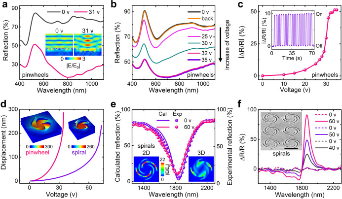
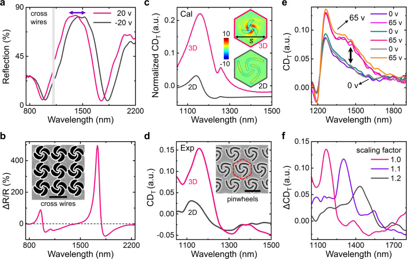
Kirigami, with facile and automated fashion of three-dimensional (3D) transformations, offers an unconventional approach for realizing cutting-edge optical nano-electromechanical systems. Here, we demonstrate an on-chip and electromechanically reconfigurable nano-kirigami with optical functionalities. The nano-electromechanical system is built on an Au/SiO2/Si substrate and operated via attractive electrostatic forces between the top gold nanostructure and bottom silicon substrate. Large-range nano-kirigami like 3D deformations are clearly observed and reversibly engineered, with scalable pitch size down to 0.975 μm. Broadband nonresonant and narrowband resonant optical reconfigurations are achieved at visible and near-infrared wavelengths, respectively, with a high modulation contrast up to 494%. On-chip modulation of optical helicity is further demonstrated in submicron nano-kirigami at near-infrared wavelengths. Such small-size and high-contrast reconfigurable optical nano-kirigami provides advanced methodologies and platforms for versatile on-chip manipulation of light at nanoscale.


Conflict of interest statement

The authors declare no competing interests.

Figures

Fig. 1
Fig. 1. Scheme for reconfigurable nano-kirigami.
a, b Schematic of a a 2D pinwheel array and b its downward 3D state under attractive electrostatic forces when the voltage is on. Each gold pinwheel is locally suspended by four SiO2 supporters with thickness of d. c A simplified electromechanical model of the reconfigurable nano-kirigami, in which the displacement of the suspended nanostructure is controlled by the downward electrostatic force (Fe) and upward mechanical restoring force (Fr). d Front-view and side-view plots of (top) 2D and (bottom) calculated 3D deformed pinwheel in the gold layer. e, f Side-view SEM images of as-fabricated 2D pinwheels and the downward deformed 3D pinwheels after applying DC voltage of V = 65 V. Structural parameters: gold thickness: t = 60 nm; pinwheel width: w = 2 µm; lattice periodicity: p = 2.25 µm; d = 500 nm. Scale bars: 1 µm.
Fig. 2
Fig. 2. Sample fabrications.
a Flow chart of the fabrication process on an Au/SiO2/Si chip. b Camera image of a pinwheel array with area of 500 × 500 μm2 before wet etching. c SEM images of i pinwheels after wet etching and ii the below SiO2 supporters after removing the top gold with FIB (Supplementary Fig. 2g). d Schematic of 2D and deformed 3D spirals in simulations. Image sizes: 2.5 × 2.5 μm2. The 2D spirals consist of four arcs with angles of (i) 180°, (ii) 270°, and (iii) 360°, respectively, which are deformed into 3D by exerting upward stresses of 3, 3, and 1 GPa in simulations. e, f SEM images of three spirals and the pinwheels after wet etching and subsequent low-dose FIB irradiation. The images agree well with simulations except the type-iii spirals, which are stuck to the bottom substrate due to the capillary force and its weak stiffness (Supplementary Fig. 3). g Top-view SEM images of 2D and deformed 3D pinwheels under V = 65 V. Corresponding side-view images are shown in Fig. 1e–f. Structural parameters: d = 300 nm in c, e, f and d = 500 nm in g. Scale bars: 1 µm.
Fig. 3
Fig. 3. Electromechanically reconfigurable optical nano-kirigami.
a Calculated and b experimental reflection spectra in normal direction for a pinwheel array under different DC voltages as noted. Inset, calculated electric field distributions in the xz-plane (y = 0) under V = 0 and 31 V (with Δd = 300 nm and λ = 750 nm), respectively. Image size: 2.5 × 2 μm2. The distorted wave shape at V = 31 V indicates the diffraction to other directions under deformations since λw (see Supplementary Fig. 6a). In experiments, the reflection stops changing when V > 32 V and the spectrum increases back to the initial 0 V condition after turning off the voltage at 35 V. c Amplitude of modulation contrast (defined as ΔR/R) versus applied voltage at λ = 750 nm. Inset, modulation contrast versus time when the voltage is turned on and off at 20 V and λ = 550 nm. d Calculated vertical displacement (Δd) versus applied voltage for a pinwheel and a type-i spiral, respectively, of which the pull-in voltages are identified at 35 and 73 V. Inset, simulated structures with corresponding maximum Δd (units: nm). e Calculated (Cal) and experimental (Exp) reflection spectra of the type-i spirals in the inset of f under V = 0 and 60 V (with Δd = 70 nm), respectively. Inset, electric field distributions of the 2D and 3D spirals in xy-plane (z= 0) at λ = 1842 nm. Image size: 1.5 × 1.5 μm2. f Modulation contrast versus wavelength when the DC voltage varies with a sequence 40 → 0 → 50 → 0 → 60 → 0 V (from bottom to top). Structural parameters: w = 2 µm, p = 2.5 µm, d = 300 nm for pinwheels; w = 1.225 µm, p = 1.5 µm, d = 300 nm for spirals. Scale bar: 1 µm.
Fig. 4
Fig. 4. Submicron nano-kirigami and reconfigurable helicity.
a Measured reflection spectra of the cross wires in the inset of b, which are switchable between V = 20 and −20 V. b Measured modulation contrast in reflection spectrum for the cross wires in the inset. Structural parameters: w = 0.796 µm, p = 0.975 µm, d = 200 nm. c, d Simulated and measured CD spectra of initial 2D and deformed 3D three-arm pinwheels [defined as CDT in arbitrary units (a.u.), see “Methods”] at V = 0 and 60 V, respectively. To compare the changes induced by 3D deformations under the same starting condition, the simulated CD spectrum of the initial 2D pattern is normalized to the experimental spectrum of the same structure. Inset of c, calculated distribution of enhancement factor of optical helicity density for 2D (left, at z = 0 plane) and deformed 3D (right, at z = −120 nm plane) pinwheels in hexagonal unit cells under RCP incidence (Supplementary Fig. 10b, c). Inset of d, SEM image of the fabricated 2D pinwheels with scaling factor of 1.0. Structural parameters: w = 0.880 µm, pinwheel spacing s = 1.15 µm, d = 300 nm. e Measured CD spectra of three-arm pinwheels with s = 1.265 μm when the voltage is switched between 0 and 65 V (see Supplementary Fig. 10f). f Measured changes in CD spectra (ΔCDT=CDT,3DCDT,2D) between 3D and 2D three-arm pinwheels under scaling factors of 1.0 (red), 1.1 (blue), and 1.2 (black). Scale bars: 1 μm.

References

    1. Collins GP. Kirigami and technology cut a fine figure, together. Proc. Natl Acad. Sci. USA. 2016;113:240–241. doi: 10.1073/pnas.1523311113. - DOI - PMC - PubMed
    1. Perks S. Flat-pack physics. Phys. World. 2015;28:21–24. doi: 10.1088/2058-7058/28/12/31. - DOI
    1. Momeni F, Hassani NSMM, Liu X, Ni J. A review of 4D printing. Mater. Des. 2017;122:42–79. doi: 10.1016/j.matdes.2017.02.068. - DOI
    1. Xu LZ, Shyu TC, Kotov NA. Origami and kirigami nanocomposites. ACS Nano. 2017;11:7587–7599. doi: 10.1021/acsnano.7b03287. - DOI - PubMed
    1. Zhang YH, et al. Printing, folding and assembly methods for forming 3D mesostructures in advanced materials. Nat. Rev. Mater. 2017;2:17019. doi: 10.1038/natrevmats.2017.19. - DOI