Review
. 2021 Sep 27;60(40):21636-21660.
doi: 10.1002/anie.202102360. Epub 2021 May 28.

Defect Passivation in Lead-Halide Perovskite Nanocrystals and Thin Films: Toward Efficient LEDs and Solar Cells

Affiliations
Review

Defect Passivation in Lead-Halide Perovskite Nanocrystals and Thin Films: Toward Efficient LEDs and Solar Cells

Junzhi Ye et al. Angew Chem Int Ed Engl. .

Abstract

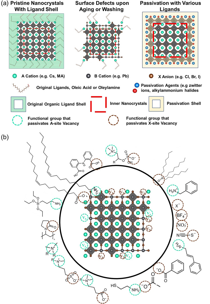
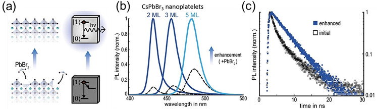
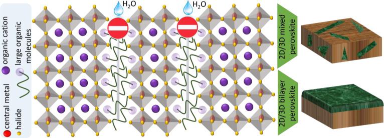
Lead-halide perovskites (LHPs), in the form of both colloidal nanocrystals (NCs) and thin films, have emerged over the past decade as leading candidates for next-generation, efficient light-emitting diodes (LEDs) and solar cells. Owing to their high photoluminescence quantum yields (PLQYs), LHPs efficiently convert injected charge carriers into light and vice versa. However, despite the defect-tolerance of LHPs, defects at the surface of colloidal NCs and grain boundaries in thin films play a critical role in charge-carrier transport and nonradiative recombination, which lowers the PLQYs, device efficiency, and stability. Therefore, understanding the defects that play a key role in limiting performance, and developing effective passivation routes are critical for achieving advances in performance. This Review presents the current understanding of defects in halide perovskites and their influence on the optical and charge-carrier transport properties. Passivation strategies toward improving the efficiencies of perovskite-based LEDs and solar cells are also discussed.

Keywords: defect passivation; lead-halide perovskites; perovskite nanocrystals; perovskite solar cells; surface chemistry.


Conflict of interest statement

The authors declare no conflict of interest.

Figures

Figure 1
Figure 1
Defects in lead‐halide perovskites. a) Types of defects in lead‐halide perovskites: i) perfect crystals, ii) A‐site vacancy, iii) X‐site vacancy, iv) B‐site vacancy, v) A‐site interstitial, vi) X‐site interstitial, vii) B‐site interstitial, viii) impurity interstitial, ix) AB anti‐sites, x) AX anti‐sites, xi) XB anti‐sites, xii) XA anti‐sites, xiii) BA anti‐sites, xiv) Bx anti‐sites, xv) lattice dislocations, xvi) grain boundary defects, xvii) Schottky defect (anion and cation vacancies occurring together), xviii) Frenkel defect (interstitial and vacancy created from the same ion), xix) impurity substitution. b) Schematic illustration of the ligand‐capped LHP nanocrystal and an enlarged view of the nanocrystal surface with defects and different types of surface ligands used for the stabilization of NCs, including alkylammonium ions, carboxylic acid, and zwitterions such as amino acids. The Figure is inspired by Ref. .
Figure 2
Figure 2
Illustration of how the electronic structure can enable defect tolerance. Left: The electronic structure of defect‐intolerant materials (e.g. silicon), in which traps primarily form deep within the band gap and have high capture cross‐sections. Right: the electronic structure of defect‐tolerant materials (e.g. MAPbI3), which primarily form shallow traps with low capture cross‐sections.
Figure 3
Figure 3
Defect tolerance in perovskite NCs. a) Effect of halide vacancies on the PLQYs of CsPbI3, CsPbBr3, and CsPbCl3 NCs, and b) transition level of halide vacancies in the band gap of these materials. Reprinted from Ref.  with permission. Copyright 2018, American Chemical Society. c) Defect diagram for CsPbI3. The dashed lines represent the conduction band minimum energies computed from GW calculations. Reprinted from Ref. [30b] with permission. Copyright 2017, American Institute of Physics.
Figure 4
Figure 4
Surface chemistry of perovskite nanocrystals and defect passivation. a) Illustration of the formation of surface defects on pristine nanocrystals with well‐capped organic ligands. Aging or washing processes will lead to ligand detachment and surface defects. Surface passivation agents are used to reform the protective shell. b) Types of passivation ligands used in perovskite nanocrystal systems. The Figure is inspired by Refs. [17a, 33].
Figure 5
Figure 5
a) UV/Vis absorption and PL spectra of pristine and treated CsPbBr3 colloidal solutions: pristine oleylamine/oleic acid stabilized NCs (black line), colloidal solution purified using acetone as a nonsolvent (containing OLA and OA; dark blue line), pristine CsPbBr3 NCs treated with a mixture of DDAB+PbBr2 (gray line), and purified colloid treated with a mixture of DDAB+PbBr2 (blue line). The inset magnifies the PL band positions of the four samples; the PL position remains unaltered after surface treatment. b) Photographs of the four colloidal solutions under illumination with UV light. The Figures are reproduced from Ref. [17a] with permission under the Creative Common CC‐BY‐NC‐ND license. Copyright 2018, American Chemical Society.
Figure 6
Figure 6
a) Schematic illustration showing the post‐synthetic surface repair of CsPbBr3 NPls by chemical treatment with a PbBr2 solution to improve their photoluminescence efficiency. b) Photoluminescence spectra of pristine (black dashed lines) and surface‐repaired (normalized, solid lines) colloidal dispersions of CsPbBr3 NPls with three different thicknesses. The enhancement clearly increases as the thickness of the NPls decrease, which suggests that the defects are more effective as the surface to volume ratio increases. c) Time‐resolved photoluminescence spectra of a 3‐monolayer NPl dispersion before (open black squares) and after surface repair (filled blue squares). (a,b,c) are reproduced from Ref. [14c] with permission the under Creative Common CC‐BY license. Copyright 2018, American Chemical Society.
Figure 7
Figure 7
a) External quantum efficiency (%) vs. emission wavelength (nm) of a perovskite light‐emitting diode. b) Radiative recombination and trap states in the dominant free charge‐carrier recombination process in bulk perovskite LEDs. Injected electrons and holes can be trapped in defects before radiatively recombining. c) Dominant exciton recombination process in quantum dot (nanocrystals) perovskite LEDs. Radiative and trap‐assisted monomolecular exciton recombination compete with each other at a low carrier density.
Figure 8
Figure 8
a) Adopting compositional engineering to reduce the formation of intrinsic material point defects. b) Passivating the intrinsic material point defects and surface defects through ligands as well as organic and inorganic salts. c) Maximizing the radiative recombination rates so that less nonradiative recombination occurs by confining the charge carriers. d) Passivating interfacial defects through interfacial engineering, such as by adding a modification layer. e) Morphology control to improve the film morphology and minimize grain boundary defects.
Figure 9
Figure 9
a) Photoluminescence quantum efficiency vs. GA doping concentration and schematic crystal structures (inset) of FA1−x GA x PbBr3 PNCs. Reproduced from Ref.  with permission. Copyright 2021, the authors, under exclusive licence to Springer Nature Limited b,c) The insets b′ and c′ show larger versions of the highlighted regions (red box). The band gap position is illustrated in purple. Reproduced from Ref. [78a] with permission. Copyright 2020, Elsevier Ltd. All rights reserved. d) Illustration of the increase in the EQE upon Ag doping. Reproduced from Ref.  with permission. Copyright 2018, American Chemical Society. e) Schematic illustration of defect passivation at perovskite grain boundaries by FPMATFA. Reproduced from Ref. [52h] with permission. Copyright 2020, WILEY‐VCH Verlag GmbH & Co. KGaA, Weinheim f,g) Structure of the QLED based on QD films without passivation (f) and with passivation (g). It is shown that TSPO1 could passivate defects on the surface of QD films, the defects may trap carriers (e.g. holes, electrons), decrease exciton recombination, and hence degrade the device performances. h) PLQY of QD films without and with TSPO1 on the bottom, on the top, and on both sides of a QD film. Error bars represent the standard deviation of experimental data for three measurements. Reproduced from Ref.  with permission under the Creative Common CC‐BY license.Copyright 2020, the authors. i) PL lifetimes for films with mixed large/small grains, small‐grains only, and large‐grains only. j) EQE as a function of time under a constant bias for perovskite LEDs with mixed large/small grains (black curve) and a normal perovskite film prepared by the vapor‐assisted two‐step method (red curve). Reproduced from Ref.  with permission under the Creative Common CC‐BY license. Copyright 2019, the authors.
Figure 10
Figure 10
Schematic illustration of a 2D/3D perovskite structure: passivation, stability, and forming the mixed and bilayer structures.
Figure 11
Figure 11
a) The proposed electronic interface in a 2D/3D mixed structure. Reproduced from Ref. [106a] with permission. Copyright 2017, Springer Nature. b) The proposed mechanism for the passivation of 3D perovskite with PEA+ ions. Reproduced from Ref. [109b] with permission. Copyright 2020, John Wiley and Sons. c) The XRD pattern of perovskite films without and with PEA+, BA+, and OA+ additives. Reproduced from Ref.  with permission. Copyright 2018, the Royal Society of Chemistry. d) Schematic chemical structure of a 5‐AVA cross‐linked perovskite structure. Reproduced from Ref.  with permission. Copyright 2017, John Wiley and Sons. e) Schematic illustration of the formation of a cross‐linked 2D/3D bilayer perovskite. Reproduced from Ref.  with permission. Copyright 2019, American Chemical Society. f) The mechanism of forming the 2D/3D bilayer structure by treatment with BA+ vapor and time‐resolved PL spectra of 3D and 2D/3D bilayer perovskites. Reproduced from Ref.  with permission. Copyright 2019, American Chemical Society.

Similar articles

Cited by

References

    1. None
    1. Queisser H. J., Haller E. E., Science 1998, 281, 945–950; - PubMed
    1. McCluskey M. D., Janotti A., J. Appl. Phys. 2020, 127, 190401;
    1. Mahajan S., Acta Mater. 2000, 48, 137–149;
    1. Pantelides S. T., Rev. Mod. Phys. 1978, 50, 797–858;

LinkOut - more resources