. 2021 Mar 19;12(1):1798.
doi: 10.1038/s41467-021-22047-w.

A flexible ultrasensitive optoelectronic sensor array for neuromorphic vision systems

Affiliations

A flexible ultrasensitive optoelectronic sensor array for neuromorphic vision systems

Qian-Bing Zhu et al. Nat Commun. .

Abstract

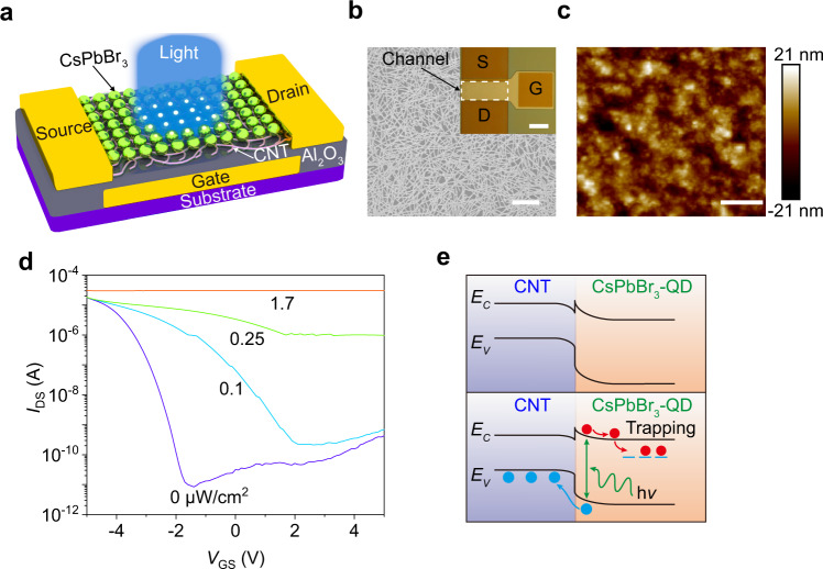
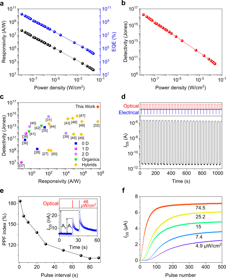
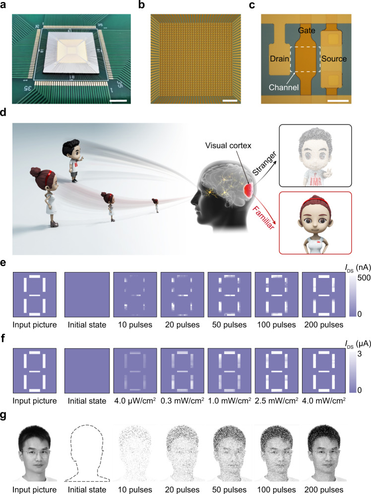
The challenges of developing neuromorphic vision systems inspired by the human eye come not only from how to recreate the flexibility, sophistication, and adaptability of animal systems, but also how to do so with computational efficiency and elegance. Similar to biological systems, these neuromorphic circuits integrate functions of image sensing, memory and processing into the device, and process continuous analog brightness signal in real-time. High-integration, flexibility and ultra-sensitivity are essential for practical artificial vision systems that attempt to emulate biological processing. Here, we present a flexible optoelectronic sensor array of 1024 pixels using a combination of carbon nanotubes and perovskite quantum dots as active materials for an efficient neuromorphic vision system. The device has an extraordinary sensitivity to light with a responsivity of 5.1 × 10⁷ A/W and a specific detectivity of 2 × 10¹⁶ Jones, and demonstrates neuromorphic reinforcement learning by training the sensor array with a weak light pulse of 1 μW/cm2.


Conflict of interest statement

The authors declare no competing interests.

Figures

Fig. 1
Fig. 1. Device design and characterization.
a Schematic of the phototransistor with a CNT/CsPbBr3-QD channel. b Scanning electron microscope (SEM) image of a CNT film (scale bar, 1 μm). Inset: optical microscope image of the fabricated device (scale bar, 50 μm). c Atomic force microscope (AFM) image of a CsPbBr3-QD film (scale bar, 250 nm). d Room temperature transfer characteristics (IDS – VGS) of the device at VDS = 1 V using a collimated incident beam of laser light with a wavelength λ of 516 nm and power densities (P) increasing from 0 to 1.7 μW/cm2. e Energy band diagram at the light-off (top panel) and light-on states (bottom panel).
Fig. 2
Fig. 2. Optoelectronic and synaptic characteristics.
a Dependence of the responsivity (R) and the external quantum efficiency (EQE) on the lighting power density (P). R=Iph/PLch×Wch, where Iph is the photocurrent, Lch and Wch are, respectively, the channel length (20 μm) and channel width (100 μm). EQE=hcR/eλ, where h is the Planck constant, c the speed of light, and e the electron charge. λ = 405 nm. b Dependence of the specific detectivity (D*) on the P. D*=RLch×Wch1/2/Sn1/2, where Sn is the noise power density (Supplementary Fig. 16). c Benchmark of the device performance demonstrating an ultra-high detectivity among reported devices made using various materials and structures. d Switching characteristics of the device under a 516 nm light with a P of 0.78 W/cm2 and a reset voltage pulse (+5 to 0 V, pulse width 100 ms) to the gate electrode. VDS = 1 V, VGS = 5 V. e PPF index decreases gradually when the pulse interval increases. Inset: PPF achieved by two successively applied optical pulses (48 μW/cm2, pulse width 20 ms, pulse interval 10 s). f Long-term potentiation with 500 optical pulses (pulse width, 20 ms; pulse interval, 500 ms) at various lighting power densities.
Fig. 3
Fig. 3. Optoelectronic sensor array.
a A sensor array chip with wire bonding on a PCB (scale bar, 5 mm). b Optical micrograph of a 32 × 32 sensor array (scale bar, 500 μm). c Magnified image of an individual sensor unit with a channel dimension of 20 × 20 μm2 (scale bar, 20 μm). d Schematics of the impression of human visual systems when strange and familiar faces are observed. e Measured training weight results of a number 8 pattern in the initial state and after training with 10, 20, 50, 100, and 200 pulses under 405 nm light with a lighting power density of 1 μW/cm2 (pulse width, 250 ms; pulse interval, 250 ms). f Measured training weight results of the sensor array after training with 10 pulses under a 405 nm light with various lighting power densities of 4.0 μW/cm2, 0.3 mW/cm2, 1.0 mW/cm2, 2.5 mW/cm2, and 4.0 mW/cm2 (pulse width, 250 ms; pulse interval, 250 ms). g Simulation results of a man’s face in the initial state and after training processes.

References

    1. Pocock DCD. Sight and knowledge. Trans. Inst. Br. Geogr. 1981;6:385–393. doi: 10.2307/621875. - DOI
    1. Kolb H. How the retina works: much of the construction of an image takes place in the retina itself through the use of specialized neural circuits. Am. Sci. 2003;91:28–35. doi: 10.1511/2003.1.28. - DOI
    1. Eldred KC, et al. Thyroid hormone signaling specifies cone subtypes in human retinal organoids. Science. 2018;362:eaau6348. doi: 10.1126/science.aau6348. - DOI - PMC - PubMed
    1. Lee GJ, Choi C, Kim DH, Song YM. Bioinspired artifcial eyes: optic components, digital cameras, and visual prostheses. Adv. Funct. Mater. 2018;28:1705202. doi: 10.1002/adfm.201705202. - DOI
    1. Ko HC, et al. A hemispherical electronic eye camera based on compressible silicon optoelectronics. Nature. 2008;454:748–753. doi: 10.1038/nature07113. - DOI - PubMed

Publication types

LinkOut - more resources