. 2021 Mar 26;7(13):eabd7921.
doi: 10.1126/sciadv.abd7921. Print 2021 Mar.

Atomic-layer-confined multiple quantum wells enabled by monolithic bandgap engineering of transition metal dichalcogenides

Affiliations

Atomic-layer-confined multiple quantum wells enabled by monolithic bandgap engineering of transition metal dichalcogenides

Yoon Seok Kim et al. Sci Adv. .

Abstract

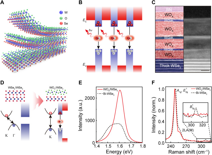
Quantum wells (QWs), enabling effective exciton confinement and strong light-matter interaction, form an essential building block for quantum optoelectronics. For two-dimensional (2D) semiconductors, however, constructing the QWs is still challenging because suitable materials and fabrication techniques are lacking for bandgap engineering and indirect bandgap transitions occur at the multilayer. Here, we demonstrate an unexplored approach to fabricate atomic-layer-confined multiple QWs (MQWs) via monolithic bandgap engineering of transition metal dichalcogenides and van der Waals stacking. The WOX/WSe2 hetero-bilayer formed by monolithic oxidation of the WSe2 bilayer exhibited the type I band alignment, facilitating as a building block for MQWs. A superlinear enhancement of photoluminescence with increasing the number of QWs was achieved. Furthermore, quantum-confined radiative recombination in MQWs was verified by a large exciton binding energy of 193 meV and a short exciton lifetime of 170 ps. This work paves the way toward monolithic integration of band-engineered heterostructures for 2D quantum optoelectronics.


Figures

Fig. 1.
Fig. 1.. Atomic–layer–confined MQWs based on monolithic bandgap engineering of WSe2.
(A) Schematic illustration of MQWs with stacking of the WOX/WSe2 hetero-bilayer as a building block. (B) Energy band diagram for MQWs consisting of the WSe2 QW (blue) and the WOX quantum barrier (red). This type I structure leads to effective carrier confinement in the QW. EC and EV indicate the conduction band edge and valence band edge, respectively. (C) Cross-sectional bright-field (left) and corresponding high-angle annular dark-field (right) STEM (scanning transmission electron microscopy) images of the triple QWs (TQWs). Scale bar, 2 nm. (D) Schematic illustration of monolithic band engineering of the bilayer WSe2, showing the transition of a band structure and energy band alignment via oxidation. (E) PL spectra and (F) Raman spectra of the layer-by-layer oxidized WOX/WSe2 hetero-bilayer and the pristine WSe2 bilayer. The inset in (F) shows the magnified B2g1 mode in Raman spectra. a.u., arbitrary units.
Fig. 2.
Fig. 2.. Analysis of the QW band structure of WOX/WSe2.
(A) PL (blue solid line) and UV-Vis absorption (green solid line) spectra of the pristine WSe2 monolayer, exhibiting the optical bandgap at 1.65 eV. (B) Tauc plot for the WOX directly oxidized from the WSe2 monolayer. The estimated bandgap is 3.28 eV. (C) UPS spectra of the secondary electron edge for the pristine WSe2 (black solid line) and the oxidized WOX (red solid line); the extracted work functions are 4.65 and 5.15 eV, respectively. (D) UPS spectra at the low binding energy region near EF for the pristine WSe2 (black solid line) and the oxidized WOX (red solid line). The energy difference of EFEV is estimated from the onset of the low binding energy, which are 1.35 and 2 eV for WSe2 and WOX, respectively. (E) Constructed band diagrams with type I band alignment between WOX and WSe2 before (left) and after (right) aligning the EF.
Fig. 3.
Fig. 3.. Optical characteristics of MQWs.
(A) Optical image (left) and spatially resolved PL map (right) of the step-like stacked MQWs. The SQW, DQWs, and TQWs areas are indicated by gray, red, and blue triangles, respectively. Scale bar, 10 μm. (B) PL spectra for the SQW (black line), DQWs (red line), and TQWs (blue line). (C) Histograms for the integrated PL intensity (left) and full width half maximum (FWHM) (right) for the SQW (gray), DQWs (red), and TQWs (blue). The integrated intensity is normalized to that of the SQW, and the values are 2.16 ± 0.96 (DQWs) and 5.31 ± 1.90 (TQWs). (D) Power-dependent PL spectra of the TQWs at 300 K. The excitation power varies from 0.09 to 120 μW. The inset shows the log scale plot of the integrated intensity as a function of power, fitted by the power law with the exponent of α = 0.96. (E) Low-frequency (left) and high-frequency (right) Raman spectra of SQW, DQWs, and TQWs.
Fig. 4.
Fig. 4.. Exciton dynamics in MQWs.
(A) Temperature-dependent PL spectra from 4 to 300 K. The red dashed line indicates the shift of the neutral exciton peak. The defect-mediated localized peak and the neutral exciton peak are denoted by Loc. and X0, respectively. (B) Plots of the X0 energy (top) and the integrated intensity (bottom) as a function of temperature. Solid black lines are fitted with the modified Varshni equation (top) and the Arrhenius equation (bottom). (C) Time-resolved PL spectra of the pristine WSe2 monolayer (black triangles) and TQWs (blue open circles) at 300 K. The curves are fitted with the biexponential decay (red solid line) for WSe2 and single-exponential decay function (purple solid line) for TQWs.

References

    1. Novoselov K. S., Mishchenko A., Carvalho A., Castro Neto A. H., 2D materials and van der Waals heterostructures. Science 353, aac9439 (2016). - PubMed
    1. Britnell L., Ribeiro R. M., Eckmann A., Jalil R., Belle B. D., Mishchenko A., Kim Y., Gorbachev R. V., Georgiou T., Morozov S. V., Grigorenko A. N., Geim A. K., Casiraghi C., Neto A. H. C., Novoselov K. S., Strong light-matter interactions thin films. Science 340, 1311–1314 (2013). - PubMed
    1. Xia F., Wang H., Xiao D., Dubey M., Ramasubramaniam A., Two-dimensional material nanophotonics. Nat. Photonics 8, 899–907 (2014).
    1. Liu X., Galfsky T., Sun Z., Xia F., Lin E., Lee Y.-H., Kéna-Cohen S., Menon V. M., Strong light–matter coupling in two-dimensional atomic crystals. Nat. Photonics 9, 30–34 (2014).
    1. Mak K. F., Lee C., Hone J., Shan J., Heinz T. F., Atomically thin MoS2: A new direct-gap semiconductor. Phys. Rev. Lett. 105, 136805 (2010). - PubMed