Review
. 2021 Mar 10;11(3):692.
doi: 10.3390/nano11030692.

Advances in Electrochemical Energy Devices Constructed with Tungsten Oxide-Based Nanomaterials

Affiliations
Review

Advances in Electrochemical Energy Devices Constructed with Tungsten Oxide-Based Nanomaterials

Wenfang Han et al. Nanomaterials (Basel). .

Abstract

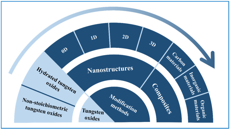
Tungsten oxide-based materials have drawn huge attention for their versatile uses to construct various energy storage devices. Particularly, their electrochromic devices and optically-changing devices are intensively studied in terms of energy-saving. Furthermore, based on close connections in the forms of device structure and working mechanisms between these two main applications, bifunctional devices of tungsten oxide-based materials with energy storage and optical change came into our view, and when solar cells are integrated, multifunctional devices are accessible. In this article, we have reviewed the latest developments of tungsten oxide-based nanostructured materials in various kinds of applications, and our focus falls on their energy-related uses, especially supercapacitors, lithium ion batteries, electrochromic devices, and their bifunctional and multifunctional devices. Additionally, other applications such as photochromic devices, sensors, and photocatalysts of tungsten oxide-based materials have also been mentioned. We hope this article can shed light on the related applications of tungsten oxide-based materials and inspire new possibilities for further uses.

Keywords: electrochromic devices; energy storage devices; multifunctional devices; tungsten oxides.


Conflict of interest statement

The authors declare no conflict of interest.

Figures

Figure 1
Figure 1
Applications of tungsten oxide-based materials for electronic devices.
Figure 2
Figure 2
(a) Tilt patterns and stability temperature domains of the different polymorphs of WO3. Reproduced with permission from [41]. Copyright IUCr Journals, 2000. The structures of hexagon phase h-WO3 shown along (b) [001] plane and (c) [100] plane. Reproduced with permission from [40]. Copyright American Chemical Society, 2009.
Figure 3
Figure 3
Structures and mechanisms of tungsten oxides working in (a) supercapacitor (SC), (b) lithium ion battery (LIB), and (c) electrochromic device (ECD). (d) Physical image of the color changing process of WO3.
Figure 4
Figure 4
(a) Initial discharge and charge curves of WO3 thin film anode. (b) SEM image of as-deposited WO3 thin film; (c) SEM and (d) selected-area diffraction (SAED) images of WO3 thin film after initially discharged to 0.01 V; (e) SEM and (f) SAED images of WO3 thin film after first charged to 4.0 V. Adapted with permission from [15]. Copyright Elsevier, 2010.
Figure 5
Figure 5
(a) High-resolution TEM image of as-prepared monodispersed tungsten oxide spherical quantum dots (QDs) with average sizes of 1.6 nm; (b) galvanostatic charge/discharge curves for QDs and bulk materials under currents of 0.2, 0.5, 1, 2, 4, 6, and 8 mA within potential from -0.5 to 0.2 V. Adapted with permission from [95]. Copyright John Wiley and Sons, 2014. High resolution SEM image (c) and cycling stability (d) of WO3 nanosheets. Adapted with permission from [69]. Copyright Elsevier, 2018.
Figure 6
Figure 6
(a) Schematic illustration of the formation, (b) FE-SEM image, (c) charge-discharge curves at 0.5 A g−1, and (c) cycling test at 10 A g−1 of the frisbee-shaped crystalline h-WO3·0.28H2O. Adapted with permission from [77]. Copyright Elsevier, 2018.
Figure 7
Figure 7
(a) Schematic illustration of the synthesis process for WOx and N-WOx; (b) high-magnification high angle annular dark field scanning transmission electron microscopy (HAADF-STEM) image of N-WOx; (c) rate performance of WOx, N-WOx, and WO3 between 0.1 A g−1 to 10 A g−1. Adapted with permission from [98]. Copyright John Wiley and Sons, 2019.
Figure 8
Figure 8
(a) Schematic illustration of the formation of hierarchical flower-like WO3·0.33H2O; (b) SEM image of WO3·0.33H2O. Adapted with permission from [101]. Copyright Society of Chemistry, 2011. (c) Schematic illustration of the formation of 3D hierarchical sandwich-type tungsten trioxide nanoplatelets and graphene (TTNPs-GS); (d) SEM overall appearance of single TTNPs-GS; (e) long cycling stability at 1080 mA g−1 for 1000 cycles of TTNPs-GS. Adapted with permission from [103]. Copyright Elsevier, 2016.
Figure 9
Figure 9
(a) Schematic illustration of the synthetic procedure, (b,c) SEM images for cauliflower-like carbon-coated WO3; (d) comparison of cycling performances of cauliflower-like WO3 and cauliflower-like carbon-coated WO3. Adapted with permission from [110]. Copyright Elsevier, 2014.
Figure 10
Figure 10
Improvements of WO3 film doped with different materials.
Figure 11
Figure 11
(a) Experiment setup for measurement of the capability of WO3/PH1000-based ECD on the modulation of solar heat; the thermal-imaging photography of the chamber under (b) bleached state and darkened state; (c) the temperature values of EC window (T1) and the back side of the chamber (T2) under bleached and darkened states. Adapted with permission from [150]. Copyright Elsevier, 2018.
Figure 12
Figure 12
(a) SEM patterns of polystyrene (PS) template and (b) ordered macroporous WO3 films; (c) optical density and (d) coloration efficiency of WO3 films and ordered macroporous films. Adapted with permission from [152]. Copyright Elsevier, 2012.
Figure 13
Figure 13
Optical transmittance spectra of the bulk m-WO3 film (a) and m-WO3-x nanowires film (b); (c) solar irradiance spectra of m-WO3-x nanowires films at 4, 2.8, 2.6 and 2 V; (d) physical photos of m-WO3-x nanowires films on ITO glasses at 4 V, 2.8 V, 2.6 V, and 2 V (vs. Li+/Li). Adapted with permission from [155]. Copyright Royal Society of Chemistry, 2014. (e) Visible-NIR spectra showing the change in absorbance when a voltage is applied on the device, between the on (i.e., negative voltage, reduced tungsten oxide) and the off (i.e., positive voltage, oxidized tungsten oxide) states at 0.5, 0.7, 0.9, 1.1, 1.3, 1.5, 1.7, and 1.9 V; (f) zoom of the spectra obtained with lower voltages. Adapted with permission from [156]. Copyright American Chemical Society, 2012.
Figure 14
Figure 14
Main modification methods of tungsten oxide-based materials applied in electrochemical applications.
Figure 15
Figure 15
(a) The galvanostatic charge-discharge profiles of the urchin-like WO3@PANI electrode at current density of 0.2 A g−1; the photographs of (b) WO3 and WO3@PANI under different voltages; (c) the durability test of the urchin-like WO3@PANI composite film for 1200 cycles at a wavelength. Adapted with permission from [174]. Copyright Springer Nature, 2010. (d) Optical density variation with respect to the charge density at 633 nm. Adapted with permission from [177]. Copyright John Wiley and Sons, 2015. (e) Basic structure and mechanism of the in situ monitoring system composed of PANI//WO3 ECSCs and CsPbBr3 perovskite photodetector. Adapted with permission from [178]. Copyright John Wiley and Sons, 2019.
Figure 16
Figure 16
Integration of electrochromic energy storing device (ECESD) with silicon-based solar cells. (a) The circuit diagram of the smart operating system; (b) from left to right, ECESD is charging by solar cell, one ECESD can independently drive an LCD screen and two ECESDs in series can lighten a red LED. Adapted with permission from [31]. Copyright American Chemical Society, 2017.
Figure 17
Figure 17
(a) Schematic diagram of the integrated system. Adapted with permission from [184]. Copyright Elsevier, 2019. (b) Schematic of charging routes for W18O49/PANI-EC battery. Adapted with permission from [187]. Copyright Elsevier, 2018.
Figure 18
Figure 18
(a) Schematic diagrams of the trifunctional device; (b) photograph of the enlarged photoelectrochromic device (PECD) at the bleached state. Adapted with permission from [30].

Similar articles

Cited by

References

    1. Divya K., Østergaard J. Battery energy storage technology for power systems—An overview. Electr. Power Syst. Res. 2009;79:511–520. doi: 10.1016/j.epsr.2008.09.017. - DOI
    1. Amrouche S.O., Rekioua D., Bacha S. Overview of energy storage in renewable energy systems. Int. J. Hydrog. Energy. 2016;41:20914–20927. doi: 10.1016/j.ijhydene.2016.06.243. - DOI
    1. González A., Goikolea E., Barrena J.A., Mysyk R. Review on supercapacitors: Technologies and materials. Renew. Sustain. Energy Rev. 2016;58:1189–1206. doi: 10.1016/j.rser.2015.12.249. - DOI
    1. Baptista J.M., Sagu J.S., Kg U.W., Lobato K. State-of-the-art materials for high power and high energy supercapacitors: Performance metrics and obstacles for the transition from lab to industrial scale—A critical approach. Chem. Eng. J. 2019;374:1153–1179. doi: 10.1016/j.cej.2019.05.207. - DOI
    1. Goodenough J.B., Park K.-S. The Li-Ion Rechargeable Battery: A Perspective. J. Am. Chem. Soc. 2013;135:1167–1176. doi: 10.1021/ja3091438. - DOI - PubMed

LinkOut - more resources