Review
. 2021 Mar 5;11(3):644.
doi: 10.3390/nano11030644.

Raman and Fluorescence Enhancement Approaches in Graphene-Based Platforms for Optical Sensing and Imaging

Affiliations
Review

Raman and Fluorescence Enhancement Approaches in Graphene-Based Platforms for Optical Sensing and Imaging

Sandra Cortijo-Campos et al. Nanomaterials (Basel). .

Abstract

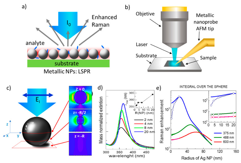
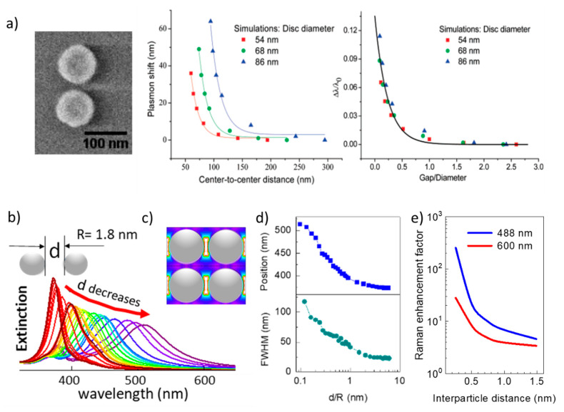
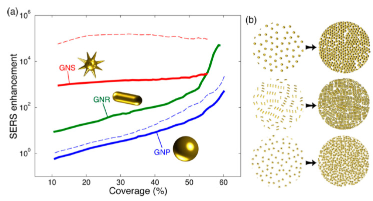
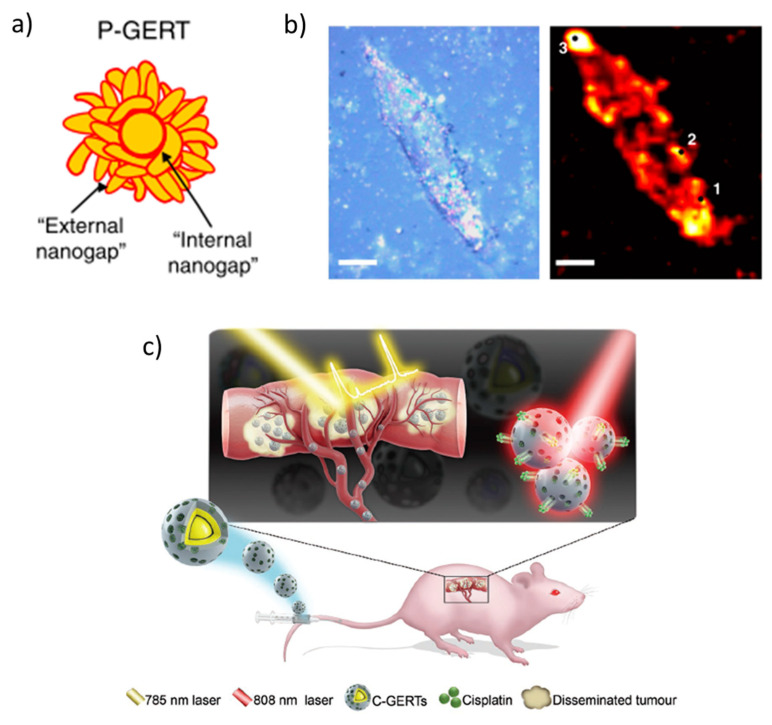
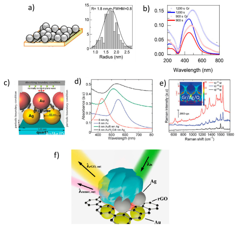
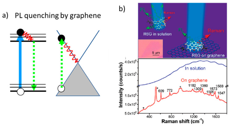
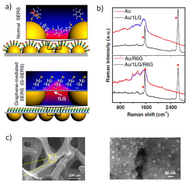
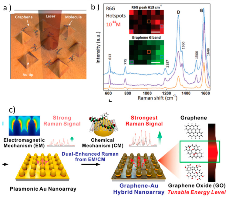
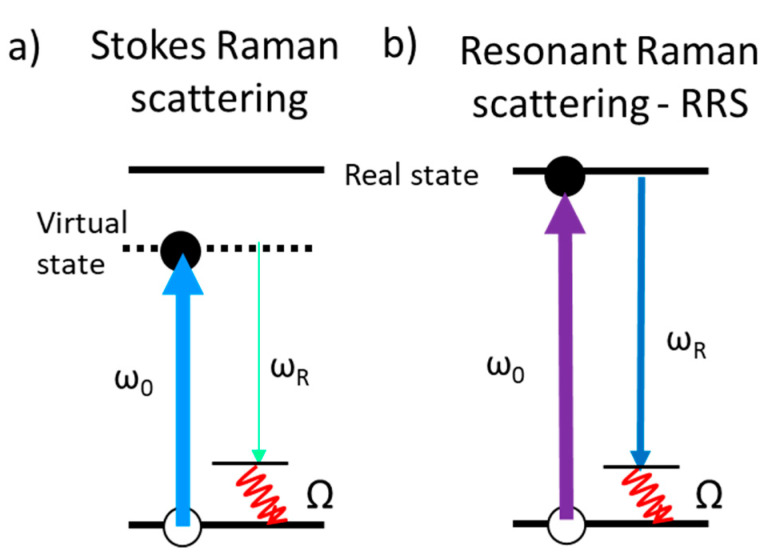
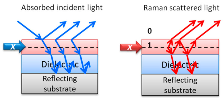
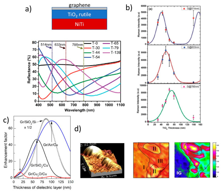
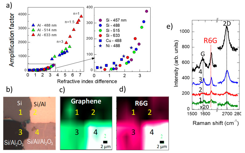
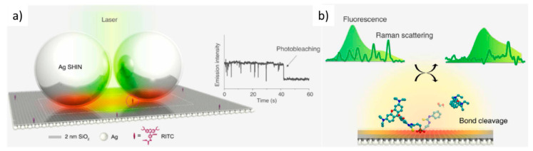
The search for novel platforms and metamaterials for the enhancement of optical and particularly Raman signals is still an objective since optical techniques offer affordable, noninvasive methods with high spatial resolution and penetration depth adequate to detect and image a large variety of systems, from 2D materials to molecules in complex media and tissues. Definitely, plasmonic materials produce the most efficient enhancement through the surface-enhanced Raman scattering (SERS) process, allowing single-molecule detection, and are the most studied ones. Here we focus on less explored aspects of SERS such as the role of the inter-nanoparticle (NP) distance and the ultra-small NP size limit (down to a few nm) and on novel approaches involving graphene and graphene-related materials. The issues on reproducibility and homogeneity for the quantification of the probe molecules will also be discussed. Other light enhancement mechanisms, in particular resonant and interference Raman scatterings, as well as the platforms that allow combining several of them, are presented in this review with a special focus on the possibilities that graphene offers for the design and fabrication of novel architectures. Recent fluorescence enhancement platforms and strategies, so important for bio-detection and imaging, are reviewed as well as the relevance of graphene oxide and graphene/carbon nanodots in the field.

Keywords: FRET; SERS; enhanced Raman scattering; enhanced fluorescence; graphene; graphene nanodots; interference; nanoparticles; optical simulations; plasmonics; resonant Raman scattering.


Conflict of interest statement

The authors declare no conflict of interest. The funders had no role in the design of the study; in the collection, analyses, or interpretation of data; in the writing of the manuscript, or in the decision to publish the results.

Figures

Figure 1
Figure 1
(a) Schema of the surface-enhanced Raman scattering (SERS) effect originated by the localized plasmon resonance of metallic inter-nanoparticles (NPs); (b) tip-enhanced Raman spectroscopy where a nanosized metal tip is used to increase the Raman signal and the spatial resolution to the nm scale; (c) inhomogeneous induced electric field at the NPs by the incident radiation with the polarization indicated by the blue arrow; (d) Mie calculations of extinction vs. Ag NP radius in the ultra-small limit normalized to the NP mass with corrected dielectric constant. Inset: plasmon resonance wavelength vs. NP radius (adapted with permissions from [32]); (e) calculated integral over the whole NP surface of the Raman enhancement as a function of the NP radius and incident laser wavelength. The inset shows the effect of considering the damping.
Figure 2
Figure 2
(a) Scanning electron microscope (SEM) image of an Au-nanodisk pair and the simulated plasmon wavelength shift vs. the inter-NP distance for three disk sizes using discrete dipole approximation (DDA) and normalized plasmon shift vs. inter-NP distance normalized to the Np diameter (adapted with permission from [46], copyright American Chemical Society, 2007). (b) Plasmon for a periodic array of 1.8 nm NPs radius (R) using finite-difference time-domain (FDTD) simulations as a function of the inter-particle distance normalized to R, from d/R = 5 to 0.1 (violet); (c) image of the electric field showing the hot-spots; (d) position and full width at half maximum (FWHM) of the plasmon in (b) as a function of d/R (adapted from [32]); (e) EF vs. inter-NP distance for 2 nm radius NPs for two excitation wavelengths.
Figure 3
Figure 3
(a) Calculated maximum SERS enhancement for different gold particle shapes vs. the coverage (fraction of an NP-monolayer) for 785 nm incident wavelength (solid lines) and (b) for a molecule-NP distance of 1 nm. Adapted with permissions from [47].
Figure 4
Figure 4
(a) Petal-like gap-enhanced Raman tag (GERT), yellow: Au, red: 4-nitrobenzenethiol (4-NBT) Raman reporter with indicated nano-gaps; (b) bright-field and Raman (1340 cm−1 NO2 vibration mode of 4-NBT) images of a single H1299 cell stained with P-GERTs, scale bars are 10 microns. Adapted with permissions from [52]. (c) Raman detection of abdominal disseminated microtumors with cisplatin-loaded GERTs. Adapted with permissions from [53]. Copyright John Wiley and Sons, 2018.
Figure 5
Figure 5
(a) Scheme of ultra-small Ag NPs deposited on graphene/quartz substrates and narrow size distribution obtained from transmission electron miscroscope (TEM) images showing an average radius of 1.8 nm; (b) absorbance of 1.8 nm NPs with two densities deposited on substrates with (open circles) and without (lines) graphene (adapted from reference [32]); (c) Au NPs/graphene/Ag NPs/quartz SERS platforms; (d) absorbance of Ag/Au (green) and Ag/graphene/Au (black); (e) Raman spectra of RhB on the 8 nm Au/1LG/8 nm Ag/Ag film/quartz for concentrations from 10−11 M to 10−13 M (adapted with permission of [80], copyright Royal Society of Chemistry, 2014) (f) Schema of the proposed mechanism for the tag-free identification and of tumor cells on Ag/rGO/Au SERS platforms. Adapted with permission of [81]. Copyright Springer Nature, 2016.
Figure 6
Figure 6
(a) Schema of the fluorescence quenching mechanism by graphene. (b) Illustration of graphene as a substrate to quench R6G fluorescence and Raman-PL spectra of R6G in water (10 µM) (blue line) and on graphene (red line) at 514 nm excitation; panel (b). Adapted with permissions from [92]. Copyright American Chemical Society, 2009.
Figure 7
Figure 7
(a) Schematic illustration of molecules with different orientations depending on whether they are adsorbed on a normal SERS substrate (gold nanoislands) or on a G-SERS substrate (graphene-coated gold hemispheres); (b) shows that the presence of graphene avoids the photo-carbonization of Au (red lines) providing cleaner spectra (black lines). The asterisks indicate the G and 2D peaks of graphene. Adapted from [94]. (c) Field enhanced SEM (FESEM) images of graphene foam at low magnification (left) and of AgNPs deposited on graphene foam substrate at high magnification (right). Adapted with permissions from [82]. Copyright Springer Nature, 2016.
Figure 8
Figure 8
(a) Schema of Au nano-pyramids (size around 200 nm) with graphene and deposited molecules; (b) Raman spectra graphene and R6G, the insets show Raman intensity images of graphene (G mode) and R6G (613 cm−1 band) demonstrating the correspondence of their intensities (scale bar is 2 µm). Adapted with permissions from [99]. Copyright John Wiley and Sons, 2013. (c) Array of almost non-interacting Au NPs fabricated by depositing an Au film on a 1 cm2 patterned substrate by laser interference lithography. A graphene oxide (GO) layer, with adjusted oxidation, is deposited on top to enhance the CM. Adapted with permissions from [100]. Copyright American Chemical Society, 2019.
Figure 9
Figure 9
(a) Standard Stokes first-order Raman scattering which results in the emission of a phonon/molecule vibration of frequency Ω and a photon of frequency ωR = ω0 − Ω with extremely low cross-section; (b) resonant Stokes Raman scattering process where the energy of the incident photons coincides with a real electronic transition, resulting in a large Raman cross-section increase.
Figure 10
Figure 10
Schemas for the interference of incident and scattered light for the simplest interference platform. The layer where the enhancement is calculated is named 1 and 0 corresponds to air.
Figure 11
Figure 11
(a) Scheme of the graphene/TiO2/NiTi interference system and the measured reflectance as a function of the TiO2 oxidation time/layer thickness; (b) G Raman peak intensity measured and calculated for three excitation wavelengths vs. the TiO2 thickness. Adapted with permission of [105], Copyright Royal Society of Chemistry, 2016. (c) Calculated enhancement factors (EF) for graphene G peak on Cu2O/Cu, SiO2/Cu, air/Cu, and SiO2/Si; (d) Atomic force microscopy (AFM) image of a graphene bubble on copper and the optical and G Raman peak Intensity images of a region with several bubbles. Adapted with permission of [107]. Copyright Elsevier, 2016.
Figure 12
Figure 12
(a) Amplification factor of G intensity for different graphene/dielectric/reflecting layer (Al (triangles), Si (circles), Cu (squares) and Ni (stars)) systems at 633 nm (red symbols), 514 nm (green), 488 nm (blue), and 457 nm (purple), laser excitation as a function of |n(dielectric) –n(reflector)|. For each reflecting material, several values of n(dielectric) ranging from 1 to 3 are calculated. (b) Optical image (20 × 20 µm) of the four zones of the heterostructure with 70 nm Al2O3 with transferred graphene and spin-coated with R6G. Raman images of the same region of (c) the 2D graphene peak and (d) the R6G 1645 cm−1 peak. (e) Representative Raman spectra of each of the four zones. Adapted with permissions from [103]. Copyright American Chemical Society, 2017.
Figure 13
Figure 13
(a) Schema of the section of a supported alumina membrane with single-layer graphene transferred on top of it. (b) SEM image of the alumina supported membrane with h ≈ 200 nm. AFM topographic images of (c) the pristine membrane and (d) after graphene transfer. (e) Image of the enhancement factor EF = I2D(membrane)/I2D (fused silica) of 2D peak of graphene on a h = 100 nm membrane. Adapted from [112].
Figure 14
Figure 14
(a) Photoluminescence process in a solid (VB = valence band, CB = conduction band, no excitonic effects are considered); fluorescence and phosphorescence processes in a molecule (HOMO = highest occupied molecular orbital, typically with S = 0). The red waves indicate phonon/vibration and vibrational relaxation; (b) fluorescence after an energy transfer from a donor molecule to an acceptor molecule. The dashed vertical arrows are virtual photons.
Figure 15
Figure 15
(a) Fluorescence spectra of GO-PEG-DVDMS at different weight ratios of GO-PEG: DVDMS; (b) in vivo distributions of GO-PEG-DVDMS and DVDMS visualized by using a molecular imaging system before and 2, 6, and 24 h after intravenous administration (DVDMS 2 mg/kg); (c) ex vivo near-infrared (NIR) fluorescence images of a tumor and major organs collected at 24 h after DVDMS or GO-PEG-DVDMS injection. Adapted with permissions from [121]. Copyright Elsevier, 2015. (d) Illustration of the (2) FTO/CS–Gr/[PSS/PDDA]3/CDs system used to enhance the CDs fluorescence and fluorescence spectra of the CDs with (2) and without (1) the reduced GO layer (CS-Gr) for the optimized poly(diallyldimethylammonium chloride)/ poly(sodium styrene sulfonate (PDDA/PSS) layer thickness. Adapted with permission from [122]. Copyright Elsevier, 2015.
Figure 16
Figure 16
(a) Overlap of donor GO quantum dots (GQD) emission and acceptor Au NPs absorption; (b) TEM images of conjugated AuNP (~15 nm) and GQDs (~3 nm); (c) Schema of the sensing mechanisms of GQDs-AuNPs Foster resonance energy transfer (FRET) biosensor for S. aureus gene detection. Adapted with permissions from [127]. Copyright Elsevier, 2015.
Figure 17
Figure 17
(a) Schema for plasmon-enhanced single-molecule spectroscopy in a plasmonic nanocavity. Right inset: emission intensity blinking behavior of a single-molecule and a single-step photobleaching event. (b) Real-time detection of the photo-induced cleavage reaction of a surface rhodamine B isothiocyanate (RITC) molecule by correlating simultaneous fluorescence and Raman signals. Adapted from [135].
Figure 18
Figure 18
Fluorescence interference enhancement of (a) R6G (#1 to #4 correspond to the four zones in (c)) and (b) single-layer MoS2. Optical images of (c) single-layer graphene (adapted with permission from [103], copyright American Chemical Society, 2017), and (d) MoS2 exfoliated flake, on interference platforms.

Similar articles

Cited by

References

    1. Wilson W.D. A technique whose time has come. Sci. Tech. Sight. 2002;295:64–65.
    1. Shao F., Zenobi R. Tip-enhanced Raman spectroscopy: Principles, practice, and applications to nanospectroscopic imaging of 2D materials. Anal. Bioanal. Chem. 2019;411:37–61. doi: 10.1007/s00216-018-1392-0. - DOI - PubMed
    1. Grant Albercht M., Alan Creighton J. Anomalously intense Raman spectra of pyridine at a silver electrode. J. Am. Chem. Soc. 1977;99:5215–5217. doi: 10.1021/ja00457a071. - DOI
    1. Stiles P.L., Dieringer J., Shah N.C., Van Duyne R.P. Surface-Enhanced Raman Spectroscopy. Annu. Rev. Anal. Chem. 2008;1:601–626. doi: 10.1146/annurev.anchem.1.031207.112814. - DOI - PubMed
    1. Sharma B., Frontiera R.R., Henry A.-I., Ringe E., Van Duyne R.P. SERS: Materials, Applications, and the Future. Mater. Today. 2012;15:16–25. doi: 10.1016/S1369-7021(12)70017-2. - DOI

LinkOut - more resources