Review
. 2021 Apr 2;10(1):72.
doi: 10.1038/s41377-021-00500-1.

Interlayer exciton formation, relaxation, and transport in TMD van der Waals heterostructures

Affiliations
Review

Interlayer exciton formation, relaxation, and transport in TMD van der Waals heterostructures

Ying Jiang et al. Light Sci Appl. .

Abstract

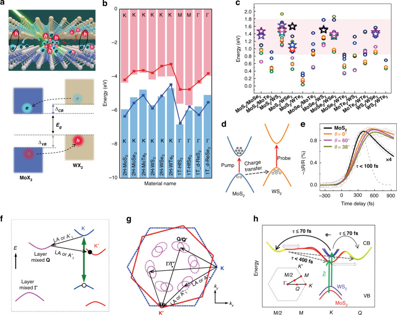
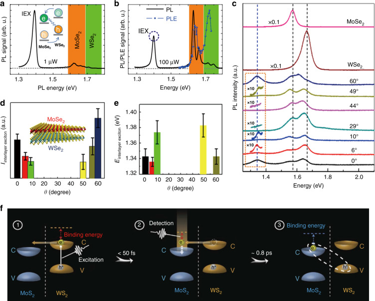
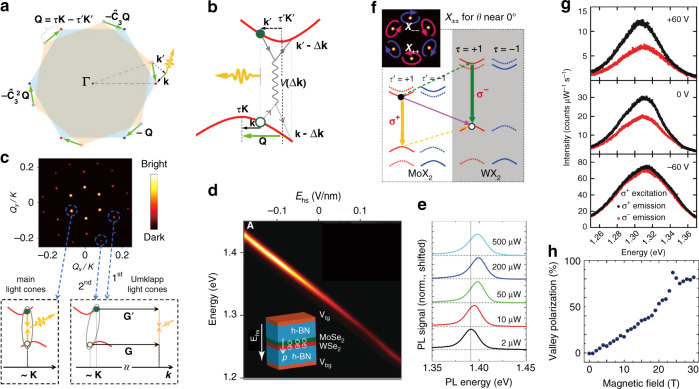
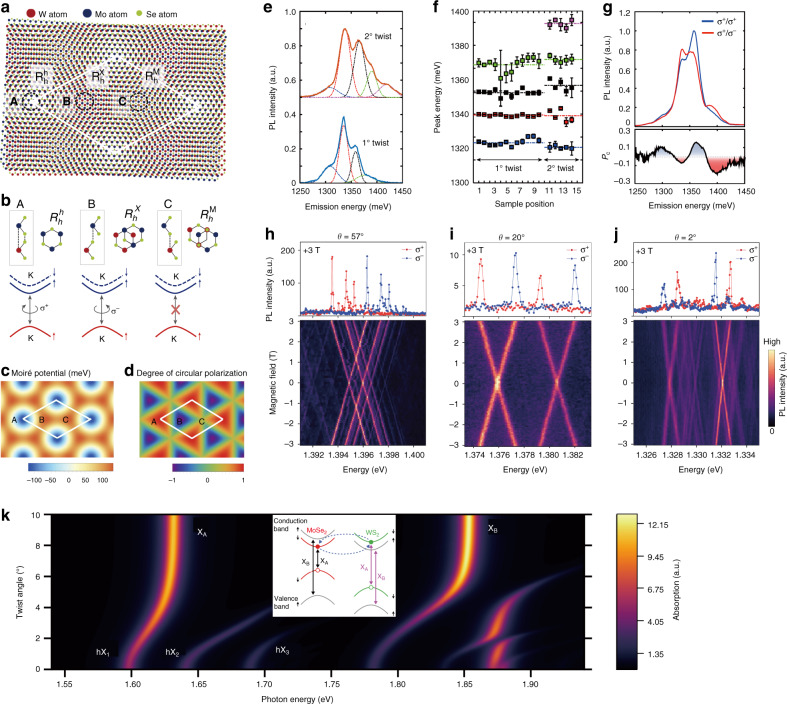
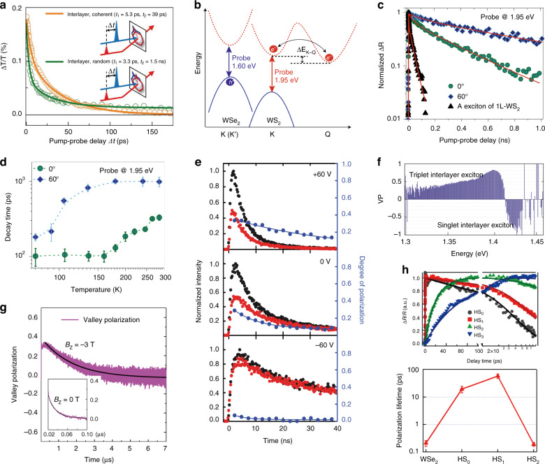
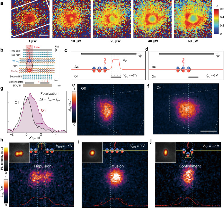
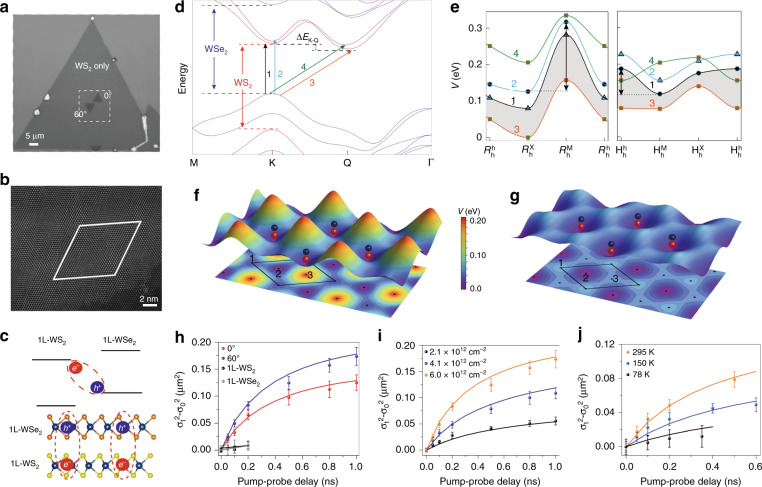
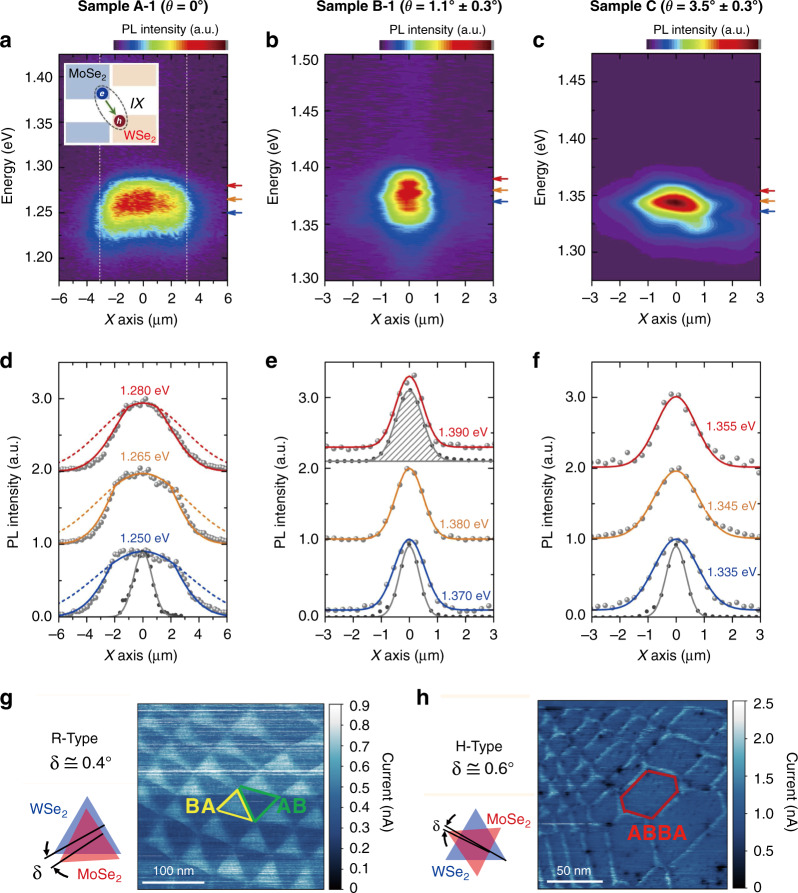
Van der Waals (vdW) heterostructures based on transition metal dichalcogenides (TMDs) generally possess a type-II band alignment that facilitates the formation of interlayer excitons between constituent monolayers. Manipulation of the interlayer excitons in TMD vdW heterostructures holds great promise for the development of excitonic integrated circuits that serve as the counterpart of electronic integrated circuits, which allows the photons and excitons to transform into each other and thus bridges optical communication and signal processing at the integrated circuit. As a consequence, numerous studies have been carried out to obtain deep insight into the physical properties of interlayer excitons, including revealing their ultrafast formation, long population recombination lifetimes, and intriguing spin-valley dynamics. These outstanding properties ensure interlayer excitons with good transport characteristics, and may pave the way for their potential applications in efficient excitonic devices based on TMD vdW heterostructures. At present, a systematic and comprehensive overview of interlayer exciton formation, relaxation, transport, and potential applications is still lacking. In this review, we give a comprehensive description and discussion of these frontier topics for interlayer excitons in TMD vdW heterostructures to provide valuable guidance for researchers in this field.


Conflict of interest statement

The authors declare no competing interests.

Figures

Fig. 1
Fig. 1. Band alignment and ultrafast charge transfer in TMD vdW heterostructures.
a Schematic illustration of the side-view structure (top) and the type-II band alignment (bottom) of a TMD vdW heterobilayer. e/h: electron/hole; ΔCB: conduction band offset of the constituent monolayers; ΔVB: valence band offset of the constituent monolayers; Eg: band gap of the heterobilayer. b Calculated band alignments of various TMD monolayers. The bar and line-point plots represent the CBM (red color) and VBM (blue color) values obtained from PBE and HSE06 calculations, respectively. The positions of CBM and VBM on the Brillouin zone are shown in the figure. c Plot of the calculated band gaps (Eg) and the experimental PL energies of the interlayer excitons versus various TMD vdW heterostructures with a type-II band alignment. The calculated Eg values (circles) are obtained from references,,–. The experimental PL energies of the interlayer excitons (stars in the pink region) are obtained from references,–,,–,,–,,,–, most of which overlap in the region from ~1.3 to ~1.5 eV. d Band alignment of a MoS2/WS2 heterobilayer. The hole transfers from the VBM of MoS2 to that of WS2 after optically pumping the MoS2 A-exciton. e Twist-angle independent charge transfer dynamics (τ < 100 fs) obtained by selectively probing the WS2 A-exciton of the MoS2/WS2 heterobilayer. f, g Schematic illustration of the phonon scattering-mediated interlayer electron transfer process in the energy (f) and momentum (g) spaces. LA (A1′) represents the longitudinal acoustic phonons. h Schematic illustration of the ultrafast electron scattering from K to M, M/2, and Q valleys within 70 fs (black arrows) in a MoS2/WS2 heterobilayer and the subsequent electron scattering from M/2 and M back to K′ and Q′ valleys in the other layer within 400 fs (dashed arrows), as evidenced by TR-ARPES. b Reprinted with permission from ref. [American Physical Society]. d, e Reprinted with permission from ref. [American Chemical Society]. f, g Reprinted with permission from ref. [American Physical Society]. h Reprinted with permission from ref. [American Physical Society]
Fig. 2
Fig. 2. Interlayer exciton formation in TMD vdW heterostructures.
a PL spectrum of the MoSe2/WSe2 heterostructure measured at 4.5 K with 1 μW excitation power. IEX represents the emissions from interlayer excitons. b PL spectrum of the MoSe2/WSe2 heterostructure (black line) measured at 4.5 K with 100 μW excitation power and the PLE spectrum (blue dots) of the interlayer exciton emission (IEX, marked by the blue dashed circle). c PL spectra of the MoSe2 monolayer, WSe2 monolayer, and MoSe2/WSe2 heterobilayer for various twist angles (0° ≤ θ ≤ 60°) at room temperature. d, e Twist-angle-dependent PL intensity (d) and energy (e) of the interlayer excitons formed in MoSe2/WSe2 heterobilayers. f Illustration of the interlayer exciton formation process in MoS2/WS2 heterostructures as revealed by transient absorption spectroscopy. a, b Reprinted with permission from ref. [IOP Publishing]. ce Reprinted with permission from ref. [American Chemical Society]. f Reprinted with permission from ref. [Springer Nature Limited]
Fig. 3
Fig. 3. Fundamental properties of interlayer excitons.
a Brillouin zone corners of the WX2 layer (τK, the solid dots) and the MoX2 layer (τ′K′, the open dots) with a small twist and/or lattice mismatch. The green arrow represents the displacement vector between the τK and τ′K′ corners of the constituent layers. C^3 is the three-fold rotational symmetry. b The electron-hole interlayer Coulomb interaction (Vk)) conserves their kinematical momentum sum Q. The interlayer exciton with a certain kinematical momentum Q equaling the momentum mismatch between the electron and hole (Q = τK−τK′, the green arrows) can recombine to emit a photon. c The main, first-Umklapp, and second-Umklapp light cones in Q space for MoSe2/WSe2 heterobilayers with twist angles θ near 0° or 60°. d PL energy of the interlayer exciton versus the electric field (Ehs) applied on the MoSe2/WSe2 heterostructure. The inset schematically displays the heterostructure cross-section. The white arrows represent the directions of the electric field (Ehs) and the static electric dipole (p). e PL spectra of the interlayer excitons in MoSe2/WSe2 heterostructures measured at 4.5 K as a function of excitation power. f Theoretically predicted valley-dependent elliptically polarized optical selection rules for interlayer excitons (X−−, X++) in the six main light cones. The dipole transition (interlayer hopping) is denoted by solid (dashed) arrows. The valley indices (τ, τ′) correspond to (+, +) or (−, −) for MoX2/WX2 heterobilayers with twist angle θ near 0°. g Circular polarization-resolved PL spectra of the interlayer exciton at selected gate voltages. All the data were obtained under σ+ circularly polarized light excitation, with the co-polarized (σ+) and cross-polarized (σ−) PL spectra shown in black and red, respectively. h Magnetic-field-dependent valley polarization of the interlayer exciton. ac, f Reprinted with permission from ref. [American Physical Society, Springer Nature Limited]. d Reprinted with permission from ref. [American Association for the Advancement of Science]. e Reprinted with permission from ref. [IOP Publishing]. g Reprinted with permission from ref. [American Association for the Advancement of Science]. h Reprinted with permission from ref. [Springer Nature Limited]
Fig. 4
Fig. 4. Moiré interlayer exciton.
a Moiré pattern in an R-type MoSe2/WSe2 heterobilayer. The three highlighted regions (A, B, and C sites) correspond to the local atomic configurations with three-fold rotational symmetry. b Side-views and top-views of the three R-type local atomic registries (A, B, and C sites) and the corresponding optical selection rules for interlayer excitons in these atomic registries. The interlayer exciton emission at the A (B) site is left-circularly (right-circularly) polarized, while that at the C site is transition-forbidden under normal incidence. c Moiré potential of the interlayer exciton transition with a local minimum at site A. d Optical selection rules for K-valley interlayer excitons. The high-symmetry A and B sites are circularly polarized with opposite signs, and the regions in between are elliptically polarized. e PL spectra of multiple moiré interlayer excitons in MoSe2/WSe2 heterobilayers with twist angles of 1° (bottom) and 2° (top). Each spectrum is fitted with four (1°) or five (2°) Gaussian functions. f The center energy of each moiré interlayer exciton resonance at different spatial positions across each sample. The average peak spacing for a twist angle of 1° (2°) is 22 ± 2 meV (27 ± 3 meV). g Circularly polarized PL spectrum of the 1° sample under σ+ excitation (top). The degree of circular polarization versus the emission wavelength is shown at the bottom, demonstrating multiple moiré interlayer excitons with alternating co-circularly and cross-circularly polarized emissions. hj Magnetic-field-dependent PL from moiré-trapped interlayer excitons in MoSe2/WSe2 heterobilayers with twist angles of 57° (h), 20° (i), and 2° (j). Top: Circular polarization-resolved PL spectra with narrow linewidth (100 μeV) at 3 T. The excitation is linearly polarized, and the σ+ and σ components of the PL emission are shown in red and blue, respectively. Bottom: total PL intensity as a function of magnetic field, displaying a linear Zeeman shift of the σ+-polarized and σ-polarized components. The derived effective g-factors from Zeeman splitting are −15.89 ± 0.02, −15.79 ± 0.05, and 6.72 ± 0.02 for samples with twist angles of 57°, 20°, and 2°, respectively. k Absorption spectrum of the MoSe2/WS2 heterobilayer as a function of the twist angle. The MoSe2 A-exciton and B-exciton resonances (XA and XB) are indicated for large twist angles where hybridization effects become negligible. The three resonances labeled hX1,2,3 appearing at θ ≈ 0° correspond to the hybridized excitons in the vicinity of XA. Those in the vicinity of XB are not labeled. Specifically, hX3 results from the hybridization of the first folding of the XA band into the mini Brillouin zone (the reduced BZ of the moiré superlattice), a direct signature of the moiré superlattice effect. ag Reprinted with permission from ref. [Springer Nature Limited]. hj Reprinted with permission from ref. [Springer Nature Limited]. k Reprinted with permission from ref. [Springer Nature Limited]
Fig. 5
Fig. 5. Population recombination and valley polarization dynamics of interlayer excitons.
a Transient dynamics of interlayer excitons at 1.6 eV in coherently stacked and randomly stacked MoS2/WS2 heterobilayers. b Schematic illustration of probing the electron (K valley of WS2 at 1.95 eV) and hole (K valley of WSe2 at 1.60 eV) dynamics in a WS2/WSe2 heterostructure using a pump energy of 1.58 eV. The hole population relates to the sum of the K–K and K–Q exciton populations, while the electron population reflects only the K–K exciton population. ΔEK–Q represents the energy difference between the lowest-energy K–Q and K–K transitions. c Electron dynamics of WS2/WSe2 heterostructures with twist angles of 0° and 60° at 295 K. The exciton dynamics of monolayer WS2 are also shown. d Electron dynamics as a function of temperature for WS2/WSe2 heterostructures with twist angles of 0° and 60°. e Co-polarized (σ+, black curves) and cross-polarized (σ, red curves) PL dynamics of interlayer excitons under σ+ excitation at selected gate voltages. The valley polarization dynamics are shown in blue curves. f Valley polarization (VP) of the singlet and triplet interlayer excitons with opposite helicities in the MoSe2/WSe2 heterobilayer. g Valley polarization dynamics of interlayer excitons in the MoSe2/WSe2 heterobilayer extending to ~μs time scale under an out-of-plane magnetic field (Bz). h Top: the interlayer exciton recombination kinetics for WS2/WSe2 heterostructures with 0, 1, 2, and 3 hBN intermediate layers, denoted HS0, HS1, HS2, and HS3, respectively; Bottom: the valley polarization lifetime in the WSe2 monolayer, HS0, HS1, and HS2. a Reprinted with permission from ref. [Macmillan Publishers Limited]. bd Reprinted with permission from ref. [Springer Nature Limited]. e Reprinted with permission from ref. [American Association for the Advancement of Science]. f Reprinted with permission from ref. [American Physical Society]. g Reprinted with permission from ref. [Springer Nature Limited]. h Reprinted with permission from ref. [American Chemical Society]
Fig. 6
Fig. 6. Interlayer exciton diffusion.
a Power dependence of the normalized PL spectra of interlayer excitons in a MoSe2/WSe2 heterobilayer. b Spatial dependence of the normalized PL intensity of interlayer excitons for different incident powers (10, 100, and 1000 μW) at 4 K. The white outlines show the MoSe2/WSe2 heterostructure area. The laser excitation spot is fixed at the top left of the sample. Scale bar, 5 μm. c Normalized PL intensity of interlayer excitons versus distance from the excitation point under different excitation powers. d Time-dependent electroluminescence (EL) intensity of the neutral (orange, ~150 ns) and charged (blue, ~25 ns) interlayer excitons in the MoSe2/WSe2 heterobilayer. e EL energy of the interlayer exciton versus the electric field (Ehs) applied vertically to the MoSe2/WSe2 heterostructure. ae Reprinted with permission from ref. [American Association for the Advancement of Science]
Fig. 7
Fig. 7. Control of the interlayer exciton transport by a laterally modulated potential landscape at room temperature.
a Schematic illustration of the MoS2/WSe2 heterostructure encapsulated in hexagonal boron nitride (h-BN) with top and bottom gates. The three gate voltages (Vg1, Vg2, and Vg3) applied to the transparent graphene electrodes (gates 1–3) can be engineered to provide a potential landscape for controlling the interlayer exciton transport through the device. b, c Calculated energy variation δE for the interlayer excitons in the ON (b free diffusion, Vg1 = Vg2 = Vg3 = 0 V) and OFF (c potential barrier, Vg1 = 16 V, Vg2 = Vg3 = 0 V) states. Red arrows represent laser excitation, and black dashed arrows denote interlayer exciton diffusion. d, e Corresponding images of the interlayer exciton emission in the ON and OFF states. Dashed lines denote the positions of the MoS2 and WSe2 monolayers and the top graphene gate (gate 1). The red circle represents the laser spot. Scale bars, 5 μm. f Calculated energy profile δE of the interlayer exciton as a function of the lateral coordinate X under the forward bias case (Vg1 = 0 V, Vg2 = 5 V, Vg3 = 10 V). The black solid lines show the direction of interlayer exciton drift. g Image of the interlayer exciton emission under the forward bias in f, demonstrating a drift distance of ~5 μm. Scale bars, 5 μm. h, i Calculated energy profile δE of the interlayer exciton for the cases of a potential well (h confinement) and a potential barrier (i, expulsion). j, k Images of the interlayer exciton emission for the potential landscapes shown in h and i. Scale bars, 5 μm. ak Reprinted with permission from ref. [Springer Nature Limited]
Fig. 8
Fig. 8. Valley-polarized interlayer exciton transport.
a Spatial map of valley polarization (ρ) of the interlayer exciton emission under 1 to 60 μW excitation. The white outline represents the sample region. Scale bar, 2 μm. b–j Valley polarized interlayer exciton transport controlled by external potential landscapes. b Schematic illustration of the interlayer exciton transistor with switch functions achieved by controlling the external gate voltages. c, d Numerically simulated energy profile (red line) of interlayer excitons in the OFF (c, a potential barrier, VTG = 0 V, VBG = − 7 V) and ON (d, free diffusion, VTG = 0 V, VBG = 0 V) states of the excitonic transistor. e, f Real-space CCD images of the interlayer exciton polarization (ΔIRL) in the OFF and ON states shown in c and d. ΔIRL = Iσ+Iσ− is the difference between the σ+ and σ circularly polarized emission intensities of the interlayer excitons. g Intensity profiles of the emitted polarization along a cutline in the middle of e and f [ref]. Scale bars, 2 μm. hj Real-space CCD images of the interlayer exciton polarization corresponding to the potential landscape configurations of repulsion (h), diffusion (i), and confinement (j). The simulated energy profile for the interlayer excitons is shown as a yellow line in the three cases. The red line shows the intensity profile along the lateral direction in the middle of the image. The red intensity profile in h is replicated as a dashed line in i and j. Insets show the PL intensity images. a Reprinted with permission from ref. [American Association for the Advancement of Science]. bj Reprinted with permission from ref. [Springer Nature Limited]
Fig. 9
Fig. 9. Interlayer exciton transport under a moiré potential.
a Optical image of two CVD-grown WS2/WSe2 heterobilayers with twist angles of 0 and 60° on the same WS2 underlayer. b High-resolution annular dark-field scanning transmission electron microscopy image of a 60° heterobilayer. The white diamond outline shows a moiré superlattice with a periodicity of ~7.6 nm. c Schematic illustration of the WS2/WSe2 heterobilayer with a type-II band alignment for facilitating interlayer exciton formation. d Schematic representation of the typical electronic band structure of a WS2/WSe2 heterobilayer in a (strained) primitive unit cell. The four lowest-energy transitions are indicated by arrows (K–K valley transitions are denoted by vertical arrows 1 and 2, and K–Q valley transitions are denoted by vertical arrows 3 and 4). The K–K transitions in individual WS2 and WSe2 monolayers are marked by vertical arrows WS2 and WSe2, respectively. e Approximate moiré potentials for twist angles of 0° (left) and 60° (right) plotted along the main diagonal of the moiré supercells (black lines in f). The spatial potential variations for 0° are much stronger (deep potential) than those for 60° (shallow potential) heterobilayers. The different lines correspond to the four lowest-energy optical transitions marked in d. f, g Illustrations of both 3D graphs and 2D projections of the 2D K-K moiré potentials for trapping interlayer excitons (red and black spheres) in local minima for 0° (f) and 60° (g) heterobilayers. A twist-angle-dependent moiré potential is indicated by the theoretical results. The numbers 1, 2, and 3 indicate the three high-symmetry local atomic registries in a moiré superlattice. h Time-dependent mean squared distances (σt2σ02) traveled by interlayer excitons in 0° and 60° heterobilayers as well as by intralayer excitons in WS2 and WSe2 monolayers (1L-WS2, 1L-WSe2). i Density-dependent interlayer exciton transport at room temperature for the 60° heterobilayer. j Temperature-dependent interlayer exciton transport for the 60° heterobilayer. aj Reprinted with permission from ref. [Springer Nature Limited]
Fig. 10
Fig. 10. Interlayer exciton diffusion at different twist angles.
ac Spatially resolved PL images of interlayer excitons in MoSe2/WSe2 heterostructures prepared by the CVD growth method (a sample A-1) and mechanical exfoliation and transfer method with a twist angle of 1.1° ± 0.3° (b sample B-1) and a twist angle of 3.5° ± 0.3° (c sample C). df PL line profiles extracted from ac for the three samples at a few selected energies. The PL line profiles for sample A-1 are truncated by the boundaries of the heterostructure region (the white dashed lines in a). The 660 nm excitation laser profile and the 900 nm laser profile are represented by the bottom gray lines and the top gray shaded area, respectively. The PL spot size of the interlayer exciton (PL wavelength near 900 nm) shown in Fig. 10e is slightly larger than the excitation laser (660 nm) spot size because of the imaging optics at different wavelengths. A Gaussian function was used to fit the measured data points. g Atomic reconstruction in the R-type MoSe2/WSe2 heterostructure with a small twist angle (δ) of ~0.4°. The yellow and green triangles represent the triangular domains with BA and AB stacking, respectively. h Atomic reconstruction in the H-type MoSe2/WSe2 heterostructure with a small twist angle (δ) of ~0.6°. The red hexagon represents the hexagonal domain with ABBA stacking. af Reprinted with permission from ref. [American Association for the Advancement of Science]. g, h Reprinted with permission from ref. [American Chemical Society]
Fig. 11
Fig. 11. Excitonic devices based on interlayer excitons.
a Polarization switching actions based on the interlayer excitons in a MoSe2/WSe2 heterostructure. ΔIRL = IRIL is the difference between the right (IR) and left (IL) circularly polarized emission intensities of the interlayer excitons. VTG is the gate voltage. b Type-II band alignment of the TMD vdW heterobilayer, forming a three-level system for lasing. c Schematic illustration of a laser device with a MoSe2/WSe2 heterobilayer integrated in a silicon nitride grating resonator. d Interlayer exciton lasing from the device in c at 5 K. The shaded boxes represent the spectral range of interlayer (IX), MoSe2, and WSe2 exciton emission. e Schematic illustration of the fabricated MoS2/WSe2 heterobilayer-PhCC nanolaser. PhCC photonic crystal cavity. f Interlayer exciton lasing from the device in e at room temperature. The linewidth is ~2.26 nm. The inset shows the spontaneous emission of the interlayer exciton for comparison. g Linewidth of the interlayer exciton emission as a function of the pump power for the laser device in e. h Light input–light output (L–L) curve showing the cavity interlayer exciton emission from the device in e with a kink, suggesting the onset of superlinear emission and lasing operation. The spontaneous emission displays a linear dependence on the pump power. i Schematic illustration of the MoSe2/WSe2 moiré heterostructure with a moiré pattern for the realization of quantum emitters. j PL spectrum of the moiré-trapped interlayer excitons formed in the MoSe2/WSe2 moiré heterostructure at 4 K. k The second-order correlation function g(2)(τ) of a single emitter at 1.401 eV shown in j. l Stark tuning of moiré-trapped interlayer excitons at different gate voltages. m Schematic illustration of the interlayer exciton photodetector based on the WS2/HfS2 heterostructure on a doped silicon substrate. n The peak responsivity of the interlayer exciton photodetector based on the WS2/HfS2 heterostructure (Vg = 0 V, Vds = −1.5 V and Idevice = 0.5 nW) and that of other reported 2D-based photodetectors in the visible and infrared range. NIR near infrared, SWIR short-wavelength infrared, MWIR mid-wavelength infrared, LWIR long-wavelength infrared, FIR far infrared. o Specific detectivity as a function of wavelength for WS2/HfS2 photodetectors shown in i and the other commercially available photodetectors at room temperature, except the one at 340 K. a Reprinted with permission from ref. [Springer Nature Limited]. bd Reprinted with permission from ref. [Springer Nature Limited]. eh Reprinted with permission from ref. [American Association for the Advancement of Science]. il Reprinted with permission from ref. [American Association for the Advancement of Science]. mo Reprinted with permission from ref. [Springer Nature Limited]

References

    1. Zeng HL, Cui XD. An optical spectroscopic study on two-dimensional group-VI transition metal dichalcogenides. Chem. Soc. Rev. 2015;44:2629–2642. doi: 10.1039/C4CS00265B. - DOI - PubMed
    1. Yu HY, et al. Valley excitons in two-dimensional semiconductors. Natl Sci. Rev. 2015;2:57–70. doi: 10.1093/nsr/nwu078. - DOI
    1. Xu XD, et al. Spin and pseudospins in layered transition metal dichalcogenides. Nat. Phys. 2014;10:343–350. doi: 10.1038/nphys2942. - DOI
    1. Mak KF, Xiao D, Shan J. Light-valley interactions in 2D semiconductors. Nat. Photonics. 2018;12:451–460. doi: 10.1038/s41566-018-0204-6. - DOI
    1. Liu YP, et al. Valleytronics in transition metal dichalcogenides materials. Nano Res. 2019;12:2695–2711. doi: 10.1007/s12274-019-2497-2. - DOI