. 2021 Jun 14;60(25):13859-13864.
doi: 10.1002/anie.202102984. Epub 2021 May 11.

A Two-Dimensional Polyimide-Graphene Heterostructure with Ultra-fast Interlayer Charge Transfer

Affiliations

A Two-Dimensional Polyimide-Graphene Heterostructure with Ultra-fast Interlayer Charge Transfer

Kejun Liu et al. Angew Chem Int Ed Engl. .

Abstract

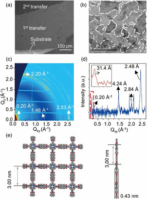
Two-dimensional polymers (2DPs) are a class of atomically/molecularly thin crystalline organic 2D materials. They are intriguing candidates for the development of unprecedented organic-inorganic 2D van der Waals heterostructures (vdWHs) with exotic physicochemical properties. In this work, we demonstrate the on-water surface synthesis of large-area (cm2 ), monolayer 2D polyimide (2DPI) with 3.1-nm lattice. Such 2DPI comprises metal-free porphyrin and perylene units linked by imide bonds. We further achieve a scalable synthesis of 2DPI-graphene (2DPI-G) vdWHs via a face-to-face co-assembly of graphene and 2DPI on the water surface. Remarkably, femtosecond transient absorption spectroscopy reveals an ultra-fast interlayer charge transfer (ca. 60 fs) in the resultant 2DPI-G vdWH upon protonation by acid, which is equivalent to that of the fastest reports among inorganic 2D vdWHs. Such large interlayer electronic coupling is ascribed to the interlayer cation-π interaction between 2DP and graphene.

Keywords: 2D polymers; graphene; interfacial synthesis; transient absorption spectroscopy; van der Waals heterostructure.


Conflict of interest statement

The authors declare no conflict of interest.

Figures

Figure 1
Figure 1
Reaction of the 2DPI by the LB method and illustration of 2DPI‐G vdWH. a) Synthesis of 2DPI on the water surface and face‐to‐face co‐assembly of graphene and 2DPI at the interface. b) Illustration of the 2DPI‐G fabrication on the water surface by LB method. There are six steps: Step 1: spread M1 onto the water surface; Step 2: well‐controlled compression induces the pre‐organization of M1; Step 3: Inject M2 into water subphase; Step 4: M2 is absorbed onto pre‐organized M1, triggering assembly and reaction; Step 5: disperse exfoliated graphene (EG) into the subphase; Step 6: 2DPI‐G formation via interfacial co‐assembly and subsequent annealing process.
Figure 2
Figure 2
Characterizations of 2DPI. a) Camera picture of the film on the water surface. b) Optical microscope image of the film with a rupture on a SiO2/Si substrate. Dash lines mark the edge of the films. c) AFM image on a SiO2/Si substrate. The height profile along the black line is inserted. d) SEM image on a copper grid with the hexagonal pores of 18 μm diameter (e) High‐resolution XPS spectrum of N 1 s region of M1 (bottom) and 2DPI (top). Nitrogen species of ‐NH2 (400.0 eV), imide (400.8 eV), and porphyrin core (including ‐N‐ at 398.4 eV and ‐NH‐ at ca. 400 eV) are marked in green, red, magenta, and violet, respectively. f) High‐resolution XPS spectrum at O1s region of M2 and 2DPI, the marked peaks at 533.18 eV (brown), and 531.58 eV (green) correspond to the character peaks of oxygen in C‐O‐C and C=O, respectively. g) ATR‐FTIR spectrum with marked reactive functional groups. h) Raman spectra of M1, M2, and 2DPI.
Figure 3
Figure 3
Morphology and structural characterization of 2DPI‐G. a) SEM image and b) low‐magnification TEM images of 2DPI‐G heterostructure after twice deposition. The edges of the graphene flakes were marked by dashed lines. c) 2D‐GIWAXS pattern of 2DPI‐G. d) The profile of integrated intensity of GIWAXS pattern with a zoom‐in view of low Qxy region. e) The model from DFT calculation, showing both top view and side view.
Figure 4
Figure 4
TEM images of the 2DPI‐G vdWHs. a) Low‐magnification TEM image. b) TEM image of the marked area in (a) clearly showing the moiré patterns. c) The zoom‐in image of the marked area in (b) shows the superlattice at higher magnification. d) Zoom‐in image of the marked area in (c) showing the crystalline lattice of EG.
Figure 5
Figure 5
Optical properties of 2DPI‐G heterostructure. a) UV/Vis absorption of monomers and 2DPI. b) Spectra of 2DPI with the different number of layers from 1 layer to 6 layers. c) The absorbance intensity of Soret bands versus layer numbers, showing a linear relationship. d) UV/Vis absorption spectra of 2DPI‐G (black) and H‐2DPI‐G (red). The spectrum of 2DPI (blue dash) is also added as the reference. e) Dynamics of transient absorption in multi‐layer graphene (blue dots), protonated 2DPI (red dots) and protonated 2DPI‐G (green dots) measured using a degenerate pump‐probe spectroscopy setup with fs pulses at 470 nm. The inset shows the sub‐ps dynamics immediately after the photoexcitation.

References

    1. None
    1. Novoselov K. S., Mishchenko A., Carvalho A., Castro Neto A. H., Science 2016, 353, aac9439; - PubMed
    1. Geim A. K., Grigorieva I. V., Nature 2013, 499, 419–425. - PubMed
    1. Xu H., Wu J., Feng Q., Mao N., Wang C., Zhang J., Small 2014, 10, 2300–2306. - PubMed
    1. Jariwala D., Sangwan V. K., Wu C. C., Prabhumirashi P. L., Geier M. L., Marks T. J., Lauhon L. J., Hersam M. C., Proc. Natl. Acad. Sci. USA 2013, 110, 18076–18080. - PMC - PubMed

LinkOut - more resources