. 2021 Apr 14;11(1):8176.
doi: 10.1038/s41598-021-87639-4.

Ultra-high critical current densities of superconducting YBa2Cu3O7-δ thin films in the overdoped state

Affiliations

Ultra-high critical current densities of superconducting YBa2Cu3O7-δ thin films in the overdoped state

A Stangl et al. Sci Rep. .

Abstract

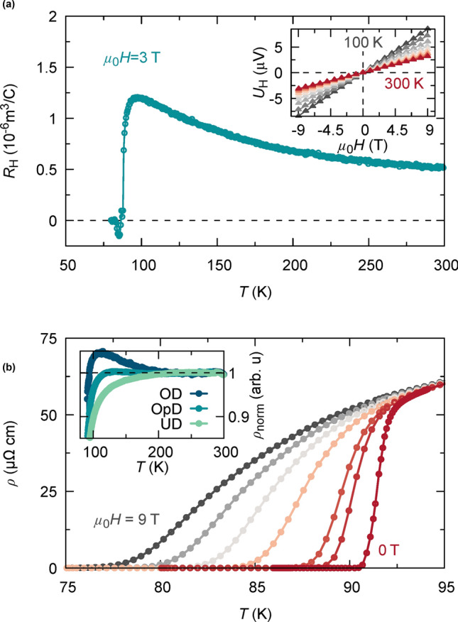
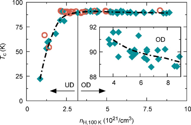
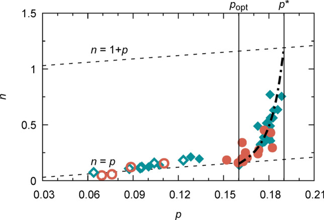
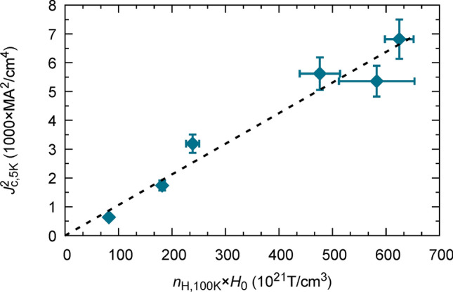
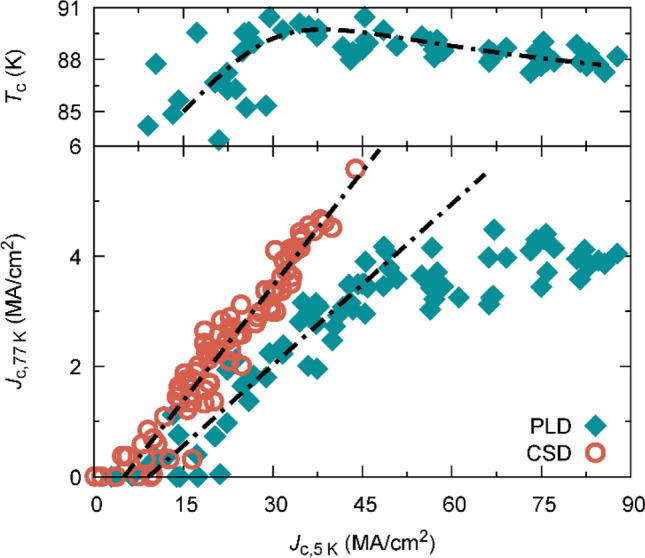
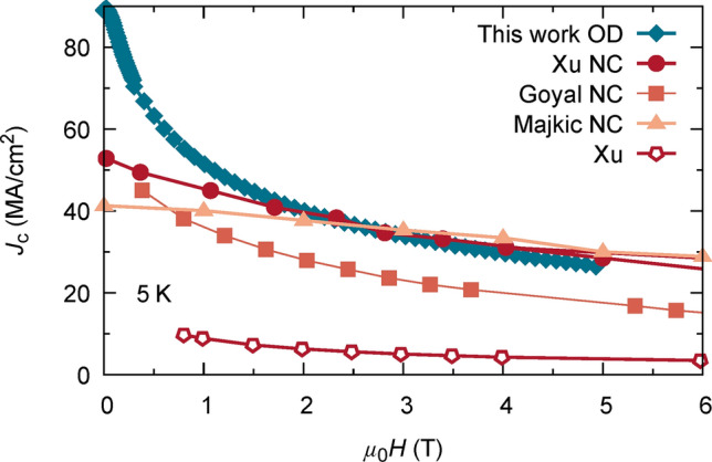
The functional properties of cuprates are strongly determined by the doping state and carrier density. We present an oxygen doping study of YBa2Cu3O7-δ (YBCO) thin films from underdoped to overdoped state, correlating the measured charge carrier density, [Formula: see text], the hole doping, p, and the critical current density, [Formula: see text]. Our results show experimental demonstration of strong increase of [Formula: see text] with [Formula: see text], up to Quantum Critical Point (QCP), due to an increase of the superconducting condensation energy. The ultra-high [Formula: see text] achieved, 90 MA cm-2 at 5 K corresponds to about a fifth of the depairing current, i.e. a value among the highest ever reported in YBCO films. The overdoped regime is confirmed by a sudden increase of [Formula: see text], associated to the reconstruction of the Fermi-surface at the QCP. Overdoping YBCO opens a promising route to extend the current carrying capabilities of rare-earth barium copper oxide (REBCO) coated conductors for applications.


Conflict of interest statement

The authors declare no competing interests.

Figures

Figure 1
Figure 1
Electrical analysis of YBCO thin films. (a) Hall constant RH obtained at 3 T as a function of temperature. RH is perfectly linear within the analysed field range (− 9 to 9 T) and vanishes in zero field condition at all T as shown in the inset. Charge carrier density is obtained via Hall effect measurements using nH(T)=1RH(T)q. (b) In-plane resistivity, ρ(T,H), as a function of temperature at different magnetic fields (0, 0.5, 1, 3, 5, 7, 9 T, Hc) to evaluate the field dependent superconducting transition temperature, T0(H). Inset shows normalized resistivity, ρnorm=(ρT-ρ0)/bT, where b is the linear slope at high temperatures (T>150K). Doping dependent deviation from unity is observed, as shown for an underdoped (UD, downwards deviation), optimally doped (OpD) and overdoped (OD, upwards bending) 200 nm thick YBCO film, respectively.
Figure 2
Figure 2
Phase diagram of YBCO thin films. Zero field critical temperature as a function of charge carrier density, nH, obtained by Hall effect measurements at 100 K for thin YBCO films grown by PLD (200 nm thick, cyan diamonds) and CSD (250 nm thick, red circles). Vertical line marks optimally doping, while arrows indicate underdoped (UD) and overdoped (OD) regime. Inset magnifies Tc in the overdoped regime, showing a weak but distinct decrease with increasing charge carrier density, from above 91 K to around 89 K.
Figure 3
Figure 3
Evolution of the charge carrier density with doping. YBCO normal state charge carrier density per CuO2-plane, n, is drawn as a function of doping p. The charge carrier density is given by n=nHV2 at 100 K. The doping p is obtained for optimally and overdoped samples (full symbols) via HR-XRD measurements of the c-parameter and for underdoped films (open symbols) from the parabolic doping dependence of Tc. The vertical lines indicate optimally and critical doping. Below popt we find n=p, corresponding to a Fermi-surface with small hole and/or electron pockets in the underdoped regime. For p>p a large, cylindrical FS is expected in the metallic overdoped regime, with n=1+p. A transition between a small and a large Fermi-surface occurs above p=0.16. This is in good agreement with previous reports, but remarkable, as within this work n is obtained by Hall effect measurements using small fields above the onset of superconductivity at 100 K.
Figure 4
Figure 4
Dependence of Jc on charge carrier density: Self-field inductive critical current density, Jc, at 5 K versus charge carrier density nH(100K) in (a) self-field and (b) an applied magnetic field of 7 T of YBCO thin films obtained by CSD (red circles, 250 nm) and PLD (cyan diamonds, 200 nm). The critical current density is determined by SQUID magnetisation measurements. Jc is strongly enhanced by increasing the charge carrier density far into the overdoped regime. Optimal and critical doping, popt and p, are marked with vertical lines, while the shadowed area around p indicates the uncertainty of defining the critical doping in terms of nH via Fig. 3. Error bars correspond to uncertainties in film thickness.
Figure 5
Figure 5
Charge carrier density dependence of superconducting parameters: (a) Characteristic magnetic field, H0, versus charge carrier density at 100 K. H0 is obtained by electrical measurements of the vortex glass transition line. It provides a measure of the pinning energy and thus is closely linked to the superconducting condensation energy, Ec. The red diamond is reproduced from (280 nm, PLD), falling on the same line as our results. Inset shows Jc5K versus H0, revealing a linear relation between these independently measured quantities. This emphasizes the strong correlation of the critical current density and the condensation energy. Dashed line is a guide to the eye. (b) Superconducting coherence length ξ(0) as a function of Hall number at 100 K. ξ(0) is obtained by electrical measurements of Hc2, determined from flux flow resistivity analysis up to 9 T (SI-Fig. 5b). A weak decrease with increasing charge carrier doping is observed, which alone cannot account for the strongly enhanced Jc in the overdoped region. y-error bars correspond to uncertainties from the underlying fit procedures.
Figure 6
Figure 6
Experimental verification of Eq. (4), Jc2nHEc, using EcH0. The three parameters Jc, nH and EC are derived experimentally, in this work, from independent measurements.
Figure 7
Figure 7
Superconducting physical properties correlations for PLD and CSD films. Tc dependence with self-field inductive Jc(5K) (upper panel) showing the intrinsic relation of both quantities with the charge carrier density. Self-field Jc(77K) as a function of self-field Jc5K for YBCO films obtained by PLD and CSD (lower panel). The different linear trends for Jc(5K)<50 MA/cm2 reveal growth dependent pinning defect landscapes, with possibly higher strong-pinning contribution in CSD films. With increasing Jc(5K) in PLD films, Jc(77K) saturates, probably due to a reduced contribution of weak pinning at high temperatures and the proximity to the superconducting transition in the overdoped regime, as indicated in the upper panel by a decreased Tc for high Jc(5K) films. All lines are guide to the eye.
Figure 8
Figure 8
Jc(Hc) at 5 K of some best performing YBCO films. Field dependence of reported high critical current densities for several nanocomposite (NC) YBCO thin films in comparison with overdoped (OD) YBCO obtained in this work (PLD). Overdoped YBCO exhibits a remarkable self-field inductive Jc, almost 60% higher than previous record films, compensating the fast decrease of Jc(H) at low fields as typical for pristine YBCO films. From literature reproduced results cover the currently best-practice strategies of nanoengineering YBCO of coated conductors: 15% Zr doped (Gd,Y)BCO (Xu NC, MOCVD, at 4.2 K, reproduced under CC-BY), nanoscale defected REBCO with 4% BZO (Goyal NC, PLD, at 5 K, reproduced under CC-BY), REBCO with 15% Zr addition (Majkic NC, MOCVD, at 4.2 K, raw data was kindly provided by the author). Additionally we show a pristine YBCO film (Xu, MOCDV, at 4.2 K, reproduced with permission from AIP publishing) as reported in.

References

    1. Rogalla H, Kes PH. 100 Years of Superconductivity. Taylor & Francis; 2011.
    1. Shiohara Y, Taneda T, Yoshizumi M. Overview of materials and power applications of coated conductors project. Jpn. J. Appl. Phys. 2012;51:010007. doi: 10.1143/JJAP.51.010007. - DOI
    1. Haugan TJ, Puig T, Matsumoto K, Wu J. Artificial pinning centers in (Y, RE)-Ba-Cu-O superconductors: Recent progress and future perspective. Supercond. Sci. Technol. 2020;33:040301. doi: 10.1088/1361-6668/ab4ccd. - DOI
    1. Obradors X, et al. Comprehensive Nanoscience and Technology. Elsevier; 2011. Nanostructured superconductors with efficient vortex pinning; pp. 303–349.
    1. Obradors X, Puig T. Coated conductors for power applications: Materials challenges. Supercond. Sci. Technol. 2014;27:044003. doi: 10.1088/0953-2048/27/4/044003. - DOI

LinkOut - more resources