

Threshold voltage instability and polyimide charging effects of LTPS TFTs for flexible displays
- PMID: 33863982
- PMCID: PMC8052436
- DOI: 10.1038/s41598-021-87950-0
Threshold voltage instability and polyimide charging effects of LTPS TFTs for flexible displays
Abstract
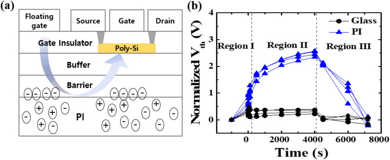
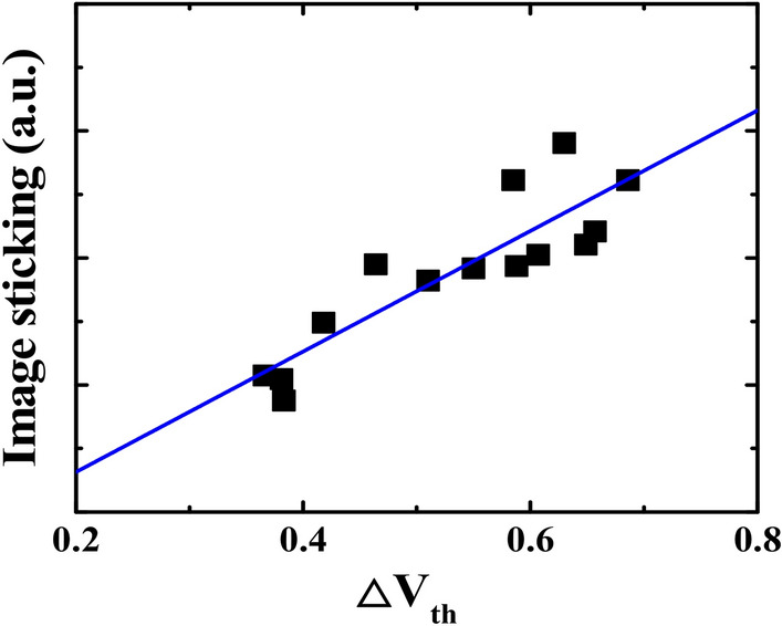
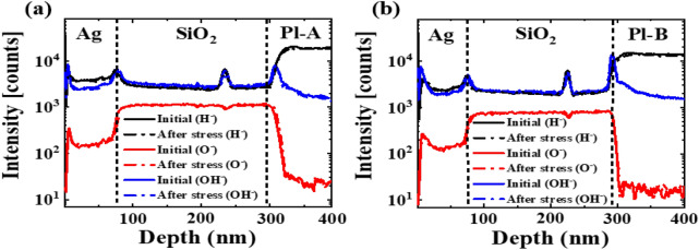
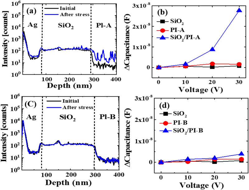
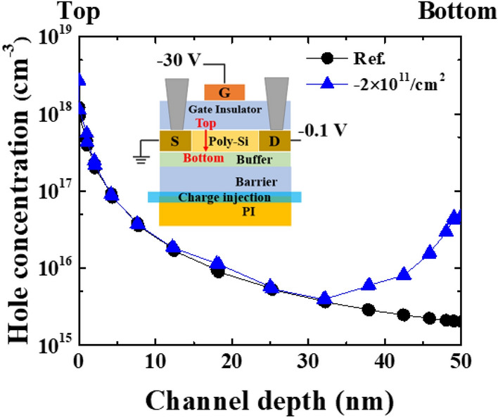
In this paper, we investigate the Vth shift of p-type LTPS TFTs fabricated on a polyimide (PI) and glass substrate considering charging phenomena. The Vth of the LTPS TFTs with a PI substrate positively shift after a bias temperature stress test. However, the Vth with a glass substrate rarely changed even with increasing stress. Such a positive Vth shift results from the negative charging of fluorine stemmed from the PI under the gate bias. In fact, the C-V characterization on the metal-insulator-metal capacitor reveals that charging at the SiO2/PI interface depends on the applied gate bias and the PI material, which agrees well with the TCAD simulation and SIMS analyses. As a result, the charging at the SiO2/PI interface contributes to the Vth shift of the LTPS TFTs leading to image sticking.
Conflict of interest statement
The authors declare no competing interests.
Figures


References
-
- Kim HJ, Im KJ, Park JW, Khim TY, Hwang HC, Kim SK, Lee SM, Song MJ, Choi PH, Song JK, Choi BD. The effects of valence band offset on threshold voltage shift in a-InGaZnO TFTs under negative bias illumination stress. IEEE Electron Dev. Lett. 2020;41:737–740. doi: 10.1109/LED.2020.2981176. - DOI
-
- Meng Z, Wang M, Wong M. High performance low temperature metal-induced unilaterally crystallized polycrystalline silicon thin film transistors for system-on-panel applications. IEEE Trans. Electron Dev. 2000;47:404–409. doi: 10.1109/16.822287. - DOI
-
- Lin CW, Cheng LJ, Lu YL, Lee YS, Cheng HC. High performance low-temperature poly-Si TFTs crystallized by excimer laser irradiation with recessed-channel structure. IEEE Electron Dev. Lett. 2001;22:269–271. doi: 10.1109/55.915606. - DOI
-
- Jin D, Lee J, Kim T, An S, Straykhilev D, Pyo Y, Kim H, Lee D, Mo Y, Kim H, Chung H. World-largest (6.5”) flexible full color top emission AMOLED display on plastic film and its bending properties. SID Symp. Tech. Dig. Pap. 2009;09:983–985. doi: 10.1889/1.3256964. - DOI
-
- Jin GH, Kim MJ. Characteristics of excimer laser-annealed thin-film transistors on the polycrystalline silicon morphology formed in the single and double (overlap) scanned area. Jpn. J. Appl. Phys. 2010;49:041301–041306. doi: 10.1143/JJAP.49.041301. - DOI
LinkOut - more resources
Full Text Sources
Other Literature Sources
Research Materials
Miscellaneous
