Review
. 2021 Feb 26;8(8):2004216.
doi: 10.1002/advs.202004216. eCollection 2021 Apr.

Recent Advances on Multivalued Logic Gates: A Materials Perspective

Affiliations
Review

Recent Advances on Multivalued Logic Gates: A Materials Perspective

Sae Byeok Jo et al. Adv Sci (Weinh). .

Abstract

The recent advancements in multivalued logic gates represent a rapid paradigm shift in semiconductor technology toward a new era of hyper Moore's law. Particularly, the significant evolution of materials is guiding multivalued logic systems toward a breakthrough gradually, whereby they are transcending the limits of conventional binary logic systems in terms of all the essential figures of merit, i.e., power dissipation, operating speed, circuit complexity, and, of course, the level of the integration. In this review, recent advances in the field of multivalued logic gates based on emerging materials to provide a comprehensive guideline for possible future research directions are reviewed. First, an overview of the design criteria and figures of merit for multivalued logic gates is presented, and then advancements in various emerging nanostructured materials-ranging from 0D quantum dots to multidimensional heterostructures-are summarized and these materials in terms of device design criteria are assessed. The current technological challenges and prospects of multivalued logic devices are also addressed and major research trends are elucidated.

Keywords: Moore's law; graphene; multivalued logic; negative differential resistances; organic semiconductors; quantum dots; transition metal dichalcogenides.


Conflict of interest statement

The authors declare no conflict of interest.

Figures

Figure 1
Figure 1
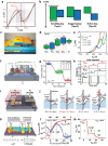
a) Projected advancements in semiconductor technology with respect to physical gate lengths for high performance logic reported in ITRS 2013, ITRS 2015, IRDS 2017 and IRDS 2020. Open circles represent the technological nodes practically realized until 2020. The inset shows the full scale view since 1970. b) Theoretical estimation of circuit complexity as a function of radix of operation. Typical input/output characteristics and figures of merit for c) binary inverter and e) STI. Temporal responses of d) binary inverter and f) STI under input voltage fluctuations.
Figure 2
Figure 2
a) Representative equivalent circuits of STIs. Schematics of transfer characteristics of component devices (top) of inverters in various configurations depicted in a) and load‐line analyses of these inverters (bottom): b) NMOS + R, c) T‐NMOS + R, d) T‐CMOS, and e) T‐NMOS + NMOS configurations. f) Load‐line analysis (top) and STI characteristics (bottom) of devices in NDR + PMOS configuration. The circuit symbol for the NDR device is that of a tunnel diode. A and B in (b)–(f) correspond to the component devices of the equivalent circuits in (a). The arrows in each figure indicate the direction in which the gate voltage increases.
Figure 3
Figure 3
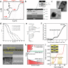
a) Transmission electron microscopy (TEM) image of two Ge2Sb2Te5 nanowires, and b) their elemental analysis (top) and spatial distributions of constituent elements (bottom). c) Variation in resistance with writing current pulse. a–c) Reproduced with permission.[ 6 ] Copyright 2008, American Chemical Society. d) Schematic of metal‐nanoparticle‐based MVL device and e) corresponding energy‐band diagram of memory device incorporated with charge‐trapping elements. f) Multilevel memory behavior in nanoparticle‐based device. d–f) Reproduced with permission.[ 5 ] Copyright 2011, Wiley. g) Schematic of electrochemically multistable molecule layer. h) Multivalued nonvolatile switching behavior. g,h) Reproduced with permission.[ 109 ] Copyright 2011, American Chemical Society.
Figure 4
Figure 4
a) Typical current–voltage characteristics of NDR device and NTC device. b) Schematic illustration of various types of band alignments. c) Structure, d) energy‐level diagram, and e) NDR characteristics of MoS2/WSe2 heterojunction device. c,e) Reproduced with permission.[ 93 ] Copyright 2015, American Chemical Society. d) The energy levels (SnSe2,[ 96 ] ReSe2,[ 52 ] MoS2,[ 94 ] WSe2,[ 96 ] and BP[ 52 ]) are adopted from the literature. f) Structure, g) STI operation, and h) SRAM operation of BP/ReS2 heterojunction device. f,g) Reproduced with permission.[ 52 ] Copyright 2016, Springer Nature. h) Reproduced with permission. Copyright 2020, Royal Society of Chemistry.[ 98 ] i) Structure and j) operating principle of pentacene/HfS2 heterojunction device.[ 99 ] k) STI device structure, l) transfer characteristics, and m) STI operation of α‐6T/PTCDI‐C8‐based AAT circuit. k–m) Reproduced with permission.[ 101 ] Copyright 2018, American Chemical Society.
Figure 5
Figure 5
a) Schematic energy‐level diagrams of p/n homojunction formed in graphene by voltage application. b) Contour map and c) current–voltage plot for NDR transfer characteristics as functions of applied biases. a,b) Reproduced with permission.[ 110 ] Copyright 2012, American Chemical Society. c) Reproduced with permission.[ 89 ] Copyright 2013, AIP Publishing. d) Device structure, e) NTC transfer characteristics, and f) STI operation of graphene transistor doped with thin metal strip. d–f) Reproduced with permission.[ 54 ] Copyright 2016, Springer Nature. g) Schematic illustration of operation of graphene transistor doped with R6G organic dye under light illumination, h) NTC transfer characteristics of device, and i) STI operation of device. g–i) Reproduced with permission.[ 105 ] Copyright 2018, American Chemical Society.
Figure 6
Figure 6
a) Schematic of three‐level transfer curve; the inset shows the circuit symbol of the T‐NMOS + R configuration. b) Device geometry of QDGFET on SOI substrate. c) TEM images of SiOx‐QD‐embedded and GeOx‐QD‐embedded structures. d) Multivalued capacitance–voltage characteristics of QDGFETs. f) Multivalued transfer characteristics of a QDGFET showing an intermediate state between the conventional on‐state and off‐state. b–f) Reproduced with permission.[ 15 , 16 ] Copyright 2011, 2015, The Institution of Engineering and Technology. g) TEM image of amorphous ZnO hybrid layer embedded with ZnO nanocrystals. h) Schematic of total density of states of hybrid nanolayer having a quantized extended state. i) Transfer characteristics of quaternary device with two intermediate states. g–i) Reproduced with permission.[ 34 ] Copyright 2019, Springer Nature.
Figure 7
Figure 7
a) Device geometry of BTBT‐based multivalued T‐CMOS transistor. b) Binary‐to‐ternary transition under scaling of applied V DD from 2 to 0.7 V. The inset shows a schematic diagram of a T‐CMOS‐based inverter. c) Photograph of 8 in wafers with T‐CMOS device arrays. a–c) Reproduced with permission.[ 53 ] Copyright 2019, Springer Nature. d) III–V semiconductor‐based nanocavity for polariton confinement. e) Multistability of polaritons. f) Trajectory of pseudospin in Bloch sphere, indicating multistability of polariton spin. d–f) Reproduced with permission.[ 108 ] Copyright 2010, Springer Nature.

References

    1. Shalf John, Philosophical Transactions of the Royal Society A: Mathematical, Physical and Engineering Sciences 2020, 378, 20190061. 10.1098/rsta.2019.0061. - DOI - PubMed
    1. Kim N. S., Austin T., Blaauw D., Mudge T., Krisztian F., Hu J. S., Irwin M. J., Kandemir M., Narayanan V., Computer 2003, 36, 68.
    1. Waldrop M. M., Nature 2016, 530, 144. - PubMed
    1. Schaller R. R., IEEE Spectrum 1997, 34, 52.
    1. Lee J.‐S., Kim Y.‐M., Kwon J.‐H., Sim J. S., Shin H., Sohn B.‐H., Jia Q., Adv. Mater. 2011, 23, 2064. - PubMed

LinkOut - more resources