Review
. 2021 Apr 28;12(5):499.
doi: 10.3390/mi12050499.

3D Manufacturing of Glass Microstructures Using Femtosecond Laser

Affiliations
Review

3D Manufacturing of Glass Microstructures Using Femtosecond Laser

Agnė Butkutė et al. Micromachines (Basel). .

Abstract

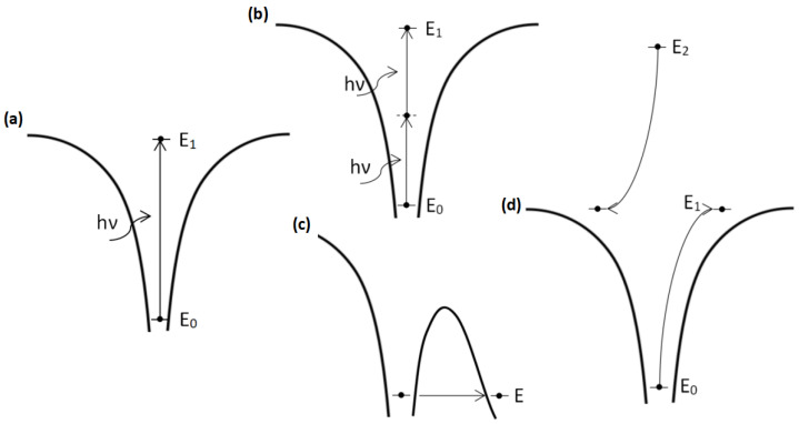
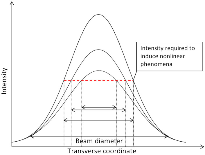
The rapid expansion of femtosecond (fs) laser technology brought previously unavailable capabilities to laser material processing. One of the areas which benefited the most due to these advances was the 3D processing of transparent dielectrics, namely glasses and crystals. This review is dedicated to overviewing the significant advances in the field. First, the underlying physical mechanism of material interaction with ultrashort pulses is discussed, highlighting how it can be exploited for volumetric, high-precision 3D processing. Next, three distinct transparent material modification types are introduced, fundamental differences between them are explained, possible applications are highlighted. It is shown that, due to the flexibility of fs pulse fabrication, an array of structures can be produced, starting with nanophotonic elements like integrated waveguides and photonic crystals, ending with a cm-scale microfluidic system with micro-precision integrated elements. Possible limitations to each processing regime as well as how these could be overcome are discussed. Further directions for the field development are highlighted, taking into account how it could synergize with other fs-laser-based manufacturing techniques.

Keywords: 3D structuring; femtosecond laser; glass micromachining.


Conflict of interest statement

The authors declare no conflict of interest.

Figures

Figure 1
Figure 1
Principle schemes of main nonlinear processes: (a) linear ionization, (b) nonlinear (multi-photon) ionization, (c) tunneling ionization and (d) avalanche ionization.
Figure 2
Figure 2
Focused laser beam spot diameter required to induce nonlinear effects dependency on radiation intensity.
Figure 3
Figure 3
Glass modification examples. (a) unmodified material, (b,c) type I of glass modification or refractive index changes. (d)—type III modification or nano/micro-voids [40].
Figure 4
Figure 4
Examples of type II glass modification and visualization of nanogratings direction dependency to light polarization. (a) Nanogratings induced with light polarization perpendicular to scanning direction- the angle between polarization and scanning direction 90°, (b) 45° and (c) 0°. (d) Nanogratings modification after etching [41].
Figure 5
Figure 5
Principle of transverse mode filtering in microchip laser by application of laser-made photonic crystal embedded in a glass chip. The solution is compact and allows to achieve a high degree of control over the spatial characteristics of a laser, depending on the geometry of inserted element. Adopted from [64].
Figure 6
Figure 6
An image depicting encoding of information using type II modification induced birefringence. While both of the images seem to be written in the same volume (image on the left) images of Maxwell (center) and Newton (right) can be separated by exploiting imaging along both optical axes. Taken from [100].
Figure 7
Figure 7
Example of microfluidic devices. (ac) nozzle for biological applications, (d) glass connector for capillary electrophoresis, diameter 15 mm, thickness 2 mm [154].
Figure 8
Figure 8
Example of microfluidic devices. (a,b) microfluidic chip created for cell sorting, (c,d) most important nodes of a chip are shown more detailed [154].
Figure 9
Figure 9
(ac) Example of a hybrid microfluidic device [160].
Figure 10
Figure 10
The precision of profile of the ultrafast laser-made axicon with subsequent CO2 polishing and comparison to commercial high-precision and standard counterparts. The un-polished and polished laser-made profiles are offset to better reveal the difference between them. Reproduced from [195].
Figure 11
Figure 11
Cross-section of the welding process (a) welding dependency on focal position. The focal position is changed in this order from image A to D: −24.1 μm, −40.0 μm, −86.5 μm and −107.3 μm, Corresponding schemes of these process are shown from picture 1 to 4, (b) welding dependency on pulse energy, the pulse energy is increasing in this order from image A to D: 10.1, 11.23, 12.9 and 18.8 μJ, schemes of the corresponding process are shown in pictures 1 to 4 [220].

References

    1. Ivey D.G., Northwood D.O. Storing energy in metal hydrides: A review of the physical metallurgy. J. Mater. Sci. 1983;18:321–347. doi: 10.1007/BF00560621. - DOI
    1. Dewidar M.M., Yoon H.C., Lim J.K. Mechanical properties of metals for biomedical applications using powder metallurgy process: A review. Met. Mater. Int. 2006;12:193–206. doi: 10.1007/BF03027531. - DOI
    1. Thames S.F., Panjnani K.G. Organosilane polymer chemistry: A review. J. Inorg. Organomet. Polym. 1996;6:59–94. doi: 10.1007/BF01098320. - DOI
    1. Merkininkaitė G., Gailevičius D., Šakirzanovas S., Jonušauskas L. Polymers for Regenerative Medicine Structures Made via Multiphoton 3D Lithography. Int. J. Polym. Sci. 2019;2019:1–23. doi: 10.1155/2019/3403548. - DOI
    1. Feng X., Qi C., Lin F., Hu H. Tungsten–tellurite glass: A new candidate medium for Yb3-doping. J. Non-Cryst. Solids. 1999;256–257:372–377. doi: 10.1016/S0022-3093(99)00476-7. - DOI

LinkOut - more resources