Review
. 2021 Apr 30;10(1):94.
doi: 10.1038/s41377-021-00527-4.

Progress on AlGaN-based solar-blind ultraviolet photodetectors and focal plane arrays

Affiliations
Review

Progress on AlGaN-based solar-blind ultraviolet photodetectors and focal plane arrays

Qing Cai et al. Light Sci Appl. .

Erratum in

Abstract

Solar-blind ultraviolet (UV) photodetectors (PDs) have attracted tremendous attention in the environmental, industrial, military, and biological fields. As a representative III-nitride material, AlGaN alloys have broad development prospects in the field of solar-blind detection due to their superior properties, such as tunable wide bandgaps for intrinsic UV detection. In recent decades, a variety of AlGaN-based PDs have been developed to achieve high-precision solar-blind UV detection. As integrated optoelectronic technology advances, AlGaN-based focal plane arrays (FPAs) are manufactured and exhibit outstanding solar-blind imaging capability. Considering the rapid development of AlGaN detection techniques, this paper comprehensively reviews the progress on AlGaN-based solar-blind UV PDs and FPAs. First, the basic physical properties of AlGaN are presented. The epitaxy and p-type doping problems of AlGaN alloys are then discussed. Diverse PDs, including photoconductors and Schottky, metal-semiconductor-metal (MSM), p-i-n, and avalanche photodiodes (APDs), are demonstrated, and the physical mechanisms are analyzed to improve device performance. Additionally, this paper summarizes imaging technologies used with AlGaN FPAs in recent years. Benefiting from the development of AlGaN materials and optoelectronic devices, solar-blind UV detection technology is greeted with significant revolutions. Summarizing recent advances in the processing and properties of AlGaN-based solar-blind UV PDs and FPAs as well as AlGaN growth and doping techniques.


Conflict of interest statement

The authors declare no competing interests.

Figures
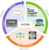
Fig. 1
Fig. 1. Diagram of this review.
Including the material section (AlGaN growth and doping), device section (AlGaN solar-blind photodetector), and application section (AlGaN focal plane array)
Fig. 2
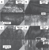
Fig. 2. Cross-sectional TEM images for the AlGaN layers grown on AlN/sapphire templates.
Samples without (a, c) and with (b, d) a 25 nm HT-GaN interlayer. a, b are measured with diffraction vector g = (0002) to image screw-component threading dislocations. c, d with g = (0–110) to image edge-component threading dislocations. The inset of Fig. 2d is an enlarged image of the dislocation, corresponding to the dashed circle. Reprinted with permission from Jiang et al.. Copyright 2005 American Institute of Physics
Fig. 3
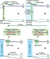
Fig. 3. Control of stress and strain during AlGaN/AlN epitaxial growth.
a Schematic diagram of relaxation process: (1) coherent growth below the critical thickness; (2) AlGaN cracks and MDs are introduced at AlGaN/GaN interface; (3) Relaxation resulted from dislocations enlarges the crack aperture; (4) cracks propagate to the GaN layer, MDs relaxing in GaN; (5) lateral growth buries cracks. Cross-sectional XTEM images of b MBE-grown AlN and c MOCVD-grown Al0.2Ga0.8N films on GaN. d SEM images of a 500-nm-thick cracked MOCVD-grown Al0.2Ga0.8N film on GaN. e Enlarged SEM image of crack overgrowth. f AFM image of a crack free Al0.2Ga0.8N film. Reprinted with permission from Bethoux et al.. Copyright 2003 American Institute of Physics
Fig. 4
Fig. 4. AlGaN/AlN superlattice employed on the AlGaN growth.
Cross-section TEM images [vector: g = (0002)] showing screw-component TDs in n-Al0.55Ga0.45N with (a) and without (b) superlattice insertion. Reprinted with permission from Sun et al.. Copyright 2005 American Institute of Physics
Fig. 5
Fig. 5. Epitaxial lateral overgrowth for AlGaN fabrication.
a Cross-sectional secondary electron image of AlGaN grown on an AlN ELO template. Reprinted with permission from Kueller et al.. Copyright 2010 Elsevier B.V. b, c SEM images of the stripe-patterned AlN/Si(111) template. d AFM image of the ELO-AlN layer grown on the patterned Si template and corresponding cross-sectional SEM image of the patterned structure (e). Atomic steps are observed over the trenches. Reprinted with permission from Cicek et al.. Copyright 2013 American Institute of Physics. f Plan-view SEM image of n-Al0.8Ga0.2N grown on ELO-AlN. g Cross-sectional annular dark-field STEM image presents that the defect distribution in the ELO-AlN-AlGaN structure. Reprinted with permission from Mogilatenko et al.. Copyright 2014 Elsevier B.V
Fig. 6
Fig. 6. Nanopatterned template for AlGaN/AlN epitaxial lateral overgrowth.
a Schematic diagram of silica nanosphere lithography. b, c SEM images of the nano-patterned substrate (NPS). d Cross-section and e plane-view SEM images of the ELO-AlN layer on the NPS. f AFM image shows the macro-steps on the AlN surface. Reprinted with permission from Donghyun et al.. Copyright 2017 American Institute of Physics. g SEM cross-sectional image of ELO-AlN nanorod pattern with air gaps. h SEM image of ELO-AlN on sapphire. Reprinted with permission from Conroy et al.. Copyright 2015 The Royal Society of Chemistry. i Coalesced AlGaN nanowire double heterostructure LED, the following two images are cross-sectional STM-HAADF image and high-magnification image, respectively. Reprinted with permission from Binh et al.. Copyright 2016 WILEY-VCH Verlag GmbH & Co. KGaA, Weinheim
Fig. 7
Fig. 7. Mg-δ-doped AlGaN layers with and without In surfactant.
a, b Mg and In concentration depth profiles. c Temperature-dependent hole concentrations. The solid lines are fitting curves. d HRXRD (0002) 2θ-ω scan curves. The inset presents the Al-content and Mg concentration depth profiles in the In-surfactant-assisted sample. e Calculated self-consistent valence band diagrams at the quantum-well and graded-barrier interface, as a result of Mg-δ-doping. Reprinted with permission from Jiang et al.. Copyright 2015 AIP Publishing LLC
Fig. 8
Fig. 8. Energy band diagrams of GaN/Al0.15Ga0.85N MQW.
a LED of N-polar QW with traditional electron blocking layer and b with graded p-AlGaN (polarization-induced p-doping). c LED of Ga-face QW: polarization fields oppose electron injection. d LED of N-face QW: polarization fields assist carrier injection. Reprinted with permission from Verma et al.. Copyright 2011 American Institute of Physics
Fig. 9
Fig. 9. Structure and performance of an AlGaN solar-blind photoconductor.
a Schematic structure of AlGaN photodetector. b Spectral responsivity of the AlGaN detector at back-illumination under 5 V bias. The insert illustrates the photocurrent resonance peak, measured at 5 V (curve 1), 12 V (curve 2), and 15 V (curve 3), respectively. c Spectral responsivity versus applied voltage ( ~ 4.8 eV). The inset presents the dark current. Vopt is the trap-free point (6 V). d Time response ( ~ 4.8 eV) at 5 V (dark circles) and 15 V (green triangles). e Time response at 5 V (trap-free regime) with 4.8 eV photon (squares) and 3.8 eV photon (triangles). f Time constant versus photon energy at 5 V. Reprinted with permission from Cherkashinin et al.. Copyright 2006 WILEY-VCH Verlag GmbH & Co. KGaA, Weinheim
Fig. 10
Fig. 10. Structure and performance of AlGaN Schottky barrier photodiodes.
a Schematic structure of Schottky AlGaN photodetector. b Responsivity of the fabricated device at 0 V. Reprinted with permission from Sang et al.. Copyright 2008 Chinese Physical Society and IOP Publishing Ltd. c Dark current of the fabricated AlGaN photodetector. d Responsivity of the devices at different applied voltages. e Pulse response of the devices at different applied voltages. f Corresponding fast Fourier transform curves. Reprinted with permission from Tut et al.. Copyright 2004 Elsevier Ltd
Fig. 11
Fig. 11. Structure and performance of a Schottky metal-semiconductor-metal photodetector.
a I-V curves of the MSM detectors measured in dark and under 254 nm UV illumination at RT and 150 °C conditions, respectively. Spectral response of the devices measured at b RT and c 150 °C. Reprinted with permission from Xie et al.. Copyright 2012 IEEE
Fig. 12
Fig. 12. Performance improvement methods on AlGaN MSM photodetectors.
a Schematic structure of AlGaN MSM photodetector with Al nanoparticles. b Electric field distribution of Al nanoparticles with changing gaps. c Responsivity of devices with and without Al nanoparticles. Reprinted with permission from Li et al.. Copyright 2014 Optical Society of America. d Schematic structure of AlGaN with low-temperature AlN cap layer and recessed electrodes. e Dark current curves of the three samples. f Spectral response of the three samples. Reprinted with permission from Chen et al.. Copyright 2010 The Japan Society of Applied Physics
Fig. 13
Fig. 13. Structures and performance of AlGaN p-i-n photodiodes.
a Schematic cross-sectional structure of p-i-n AlGaN photodetector. b I-V curves of ten devices on the same wafer. Turn-on voltage is 5.6 V. The label shows series resistance and ideality factor. c Responsivity at different reverse biases. 176 mA/W under zero bias and 192 mA/W at 5 V. Reprinted with permission from Cicek et al.. Copyright 2013 AIP Publishing LLC. d Schematic cross-sectional structure of the photodetector. e I-V curves at different temperatures. f Responsivity at various biases. The inset illustrates quantum efficiency in the wavelength range from 250 to 300 nm. Reprinted with permission from Wang et al.. Copyright 2012 Chinese Physical Society and IOP Publishing Ltd
Fig. 14
Fig. 14. Structure and performance of an AlGaN SAM APD.
a Schematic cross-sectional diagram of the SAM AlGaN APD. b I-V curve in dark and under illumination. Sidewall SEM images of APD with KOH (c) and photo-electrochemical (d) treatment, respectively. e Dark currents for samples with different treatments. f Spectral response at various applied voltages. g Dark currents at various temperatures. Reprinted with permission from Shao et al.. Copyright 2014 IEEE
Fig. 15
Fig. 15. Polarization engineering for improving device performance.
Schematic structures of various back-illuminated SAM APDs: a simulated polarization-enhanced, d, e conventional counterpart and experimental polarization-enhanced, g ionization-enhanced. b, f, h The I-V and gain curves of the proposed APDs, respectively, transverse corresponding. c Electric field distribution of sample a. i EQE of sample g. Reprinted with permission from Dong et al. and Shao et al.,. Copyright 2013 IEEE, 2014 IEEE and 2017 IEEE
Fig. 16
Fig. 16. Hybrid-packaged AlGaN focal plane arrays.
Indium bump for FPA interconnect AlGaN solar-blind UV photodetector with silicon ROIC
Fig. 17
Fig. 17. 256 × 256 AlGaN UV FPA structure and imaging.
a Schematic cross-sectional diagram of AlGaN-based FPA structure. b UV reflection image of a US dollar coin with the fabricated FPA. Reprinted with permission from Lamarre et al.. Copyright WILEY-VCH Verlag Berlin GmbH
Fig. 18
Fig. 18. 320 × 256 AlGaN UV FPAs and imaging technology.
a Schematic structure of the AlGaN photodetector. b Spectral response at 0 V. c Electrical arc discharge image from FPA camera. d Paper-cutout image from FPA camera. e SEM image of FPA with indium bump. f Schematic diagram of Imaging geometry. Reprinted with permission from McClintock et al.. Copyright 2005 SPIE
Fig. 19
Fig. 19. AlGaN p-i-n solar-blind UV FPAs and imaging by Nanjing University.
a 320 × 256 AlGaN FPAs on 2-inch sapphire wafer. b Optical images of AlGaN focal plane arrays. c I-V characteristics of individual photodetector. d Silicon driver IC. e Optical images of array with Indium bumps. f Solar-blind ultraviolet images taken from the AlGaN FPA camera
Fig. 20
Fig. 20. Reduced area epitaxy for the growth of AlGaN photodetector pixels.
a SEM image of patterned AlN, mesa size: 26 μm × 26 μm, periodicity: 30 μm. b Cross-sectional SEM image of sidewall. Implemented AlGaN UV photodetector grown on patterned (c) and unpatterned (d) AlN template. Reprinted with permission from Cicek et al.. Copyright 2013 American Institute of Physics

References

    1. Shibata T, et al. Evaluation of the solar-blind effect in ultraviolet ozone lidar with raman lasers. Appl. Opt. 1987;26:2604–2608. - PubMed
    1. McClintock, R. et al. AlxGa1-xN materials and device technology for solar blind ultraviolet photodetector applications. In Proc. of SPIE 4288, Photodetectors: Materials and Devices VI. 219–229 (SPIE, San Jose, 2001).
    1. Safin RG, et al. Solar-blind filter for the ultraviolet region. J. Opt. Technol. 2007;74:208–210.
    1. Kuryatkov V, et al. Solar-blind ultraviolet photodetectors based on superlattices of Aln/Alga(in)N. Appl. Phys. Lett. 2003;82:1323–1325.
    1. Reilly, D. M., Moriarty, D. T. & Maynard, J. A. Unique properties of solar blind ultraviolet communication systems for unattended ground-sensor networks. In Proc. of SPIE 5611, Unmanned/Unattended Sensors and Sensor Networks. 244–254 (SPIE, London, 2004).