. 2021 May 5;12(1):2542.
doi: 10.1038/s41467-021-22774-0.

Tunneling current modulation in atomically precise graphene nanoribbon heterojunctions

Affiliations

Tunneling current modulation in atomically precise graphene nanoribbon heterojunctions

Boris V Senkovskiy et al. Nat Commun. .

Abstract

Lateral heterojunctions of atomically precise graphene nanoribbons (GNRs) hold promise for applications in nanotechnology, yet their charge transport and most of the spectroscopic properties have not been investigated. Here, we synthesize a monolayer of multiple aligned heterojunctions consisting of quasi-metallic and wide-bandgap GNRs, and report characterization by scanning tunneling microscopy, angle-resolved photoemission, Raman spectroscopy, and charge transport. Comprehensive transport measurements as a function of bias and gate voltages, channel length, and temperature reveal that charge transport is dictated by tunneling through the potential barriers formed by wide-bandgap GNR segments. The current-voltage characteristics are in agreement with calculations of tunneling conductance through asymmetric barriers. We fabricate a GNR heterojunctions based sensor and demonstrate greatly improved sensitivity to adsorbates compared to graphene based sensors. This is achieved via modulation of the GNR heterojunction tunneling barriers by adsorbates.


Conflict of interest statement

The authors declare no competing interests.

Figures

Fig. 1
Fig. 1. Electronic structure of GNR heterojunctions.
a Schematic illustration of the aligned GNR heterojunctions integrated into the device. Lateral fusion of 7-AGNRs leads to the formation of quasi-metallic 14-AGNR and 21-AGNRs. When the source–drain contacts are fabricated, the remaining 7-AGNR segments act as tunneling barriers. Red arrows indicate different paths for charge transport. b Potential U(x) as a function of coordinate x between source and drain contacts of multiple 7-/14-AGNR heterojunctions. The Fermi level EF, the barrier height Φb, and the barrier length d are indicated. The Fermi function shows the distribution of electrons in 14-AGNRs. Thermionic emission (red arrow) and tunneling (blue arrow) mechanisms are schematically shown. c, d Sketch of the electronic energy band dispersions of 7-AGNR and 14-AGNR. Momentum along the ribbon axis is denoted as k. The conduction and valence band edges are CB1 and VB1, respectively, and determine the value of Φb.
Fig. 2
Fig. 2. Experimental characterization of the aligned GNR heterojunctions on Au(788).
a STM topographic image of fused 7-AGNRs (sample bias Vs = −1.3 V, tunneling current It = 1.8 nA). The black lines outline one possible conducting path through the GNR heterojunctions: quasi-metallic 14- and 21-AGNRs connected by 7-AGNR segments. The inset shows an example of a typical 14-/7-/14-AGNR heterojunction with a short (~3 nm) 7-AGNR segment. See also Supplementary Note 1. b Calculated electronic band structure of 7-AGNRs (blue) and 14-AGNRs (red) shown in the second Brillouin zone of GNRs, where the ARPES scans were acquired. The first and the second valence sub-bands of 14-AGNRs (7-AGNRs) are labeled as VB114-AGNR (VB17-AGNR) and VB214-AGNR (VB27-AGNR), respectively. The valence band maxima in the calculations are aligned to the ARPES data. c Second derivative with respect to momentum of the ARPES scan (to enhance the contrast) of fused GNRs on Au(788) measured along the GNR axis (k) with fixed in-plane momentum perpendicular to the axis (k). To maximize the photoemission intensity from VB114-AGNR, we used k = 1.1 Å−1. At this k, the intensities from VB214-AGNR and VB27-AGNR overlap (Supplementary Note 2). The Au sp bands that are from the substrate are also indicated. d UHV Raman spectra (300 K, 633 nm) of GNRs on Au(788) before and after fusion. The frequencies of the respective Raman peaks are indicated (values in cm−1). e Calculated Raman spectra of 7-AGNR and 14-AGNR. The structure of 7-AGNR and 14-AGNR unit cells with the eigenvectors of selected phonon modes are shown (see also Supplementary Note 4). The arrows indicate the atomic displacement. The RBLM37 and RBLM314 are the third overtones of RBLM7 and RBLM14, respectively.
Fig. 3
Fig. 3. Charge transport characterization of the transferred GNR heterojunctions.
a Top: scanning electron microscopy image of the device with the channel length L = 200 nm and the channel width W = 25 μm. Bottom: sketch of aligned GNR heterojunctions on SiO2/Si in a FET geometry with source, drain, and gate contacts. bd Transport characteristics of the device with L = 200 nm. b IdVd curves at different Vg, and c Id versus Vg at different Vd at 4 K. d IdVd curves in log scale at 4 K (blue) and room temperature (red) at Vg = 0 and −70 V. e Channel length dependence of the Id at Vd = 8 V and different Vg at room temperature.
Fig. 4
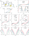
Fig. 4. Comparison of experimental and calculated IdVd curves.
a The energy diagram along one conducting channel of GNR heterojunctions. The tunneling through a barrier (blue arrows) followed by relaxation of the carrier (green arrows) is illustrated. The Fermi level of the nth barrier is indicated as EF,n. The energy drop across one barrier, equal to eV = eVd/M (where e is the electron charge and M is the number of barriers in the channel), is indicated along with the barrier height Φb and the barrier length d. b Sketch of log(Id) versus Vd characteristics of three different barriers. At high Id, the voltage drops Vd across the barriers assume a narrower distribution (indicated by horizontal arrows). c Experimental (empty circles) and calculated (solid lines) IdVd curves of the 350 nm channel device at different temperatures between 4 and 295 K at Vg = 0. The inset shows the IdVd curves in a log scale. df Experimental (empty circles) and calculated (solid lines) IdVd curves for devices with L = 300, 500, and 700 nm at Vg = −10, −30, and −50 V at 295 K in linear (top) and log (bottom) scales. The inset in f shows the M versus L dependence and its linear fit.
Fig. 5
Fig. 5. Band structure and charge transport of Li-doped GNR heterojunctions.
a Sketch of the experimental set-up containing a Li source and the GNR heterojunction FET mounted on a UHV compatible sample holder. b Sketch of the band structure changes of 14-AGNRs upon Li doping. c Second derivatives of ARPES scans by momentum of the GNR heterojunctions on Au(788) before (left) and after (right) Li deposition (~1 Å) at k = 0.71 Å−1 (Supplementary Note 3). Dashed vertical white line denotes the center of the second Brillouin zone of AGNRs. Red dashed lines are the calculated electronic band structure, aligned in energy to the ARPES data. d IdVd characteristics before (pristine sample) and after deposition of three identical Li doses (~0.1 Å each) in linear and log (inset) scales for the L = 200 nm device. Experimental points (exp.) are shown by circles, the fit is indicated by solid lines. e Schematic illustration of the potential profile U(x) across a tunneling barrier for pristine and Li-doped GNR heterojunctions. f The ratio (log scale) of current after Li doping Id to the current in pristine sample Id0 for three Li doses for the L = 200 nm device at Vd = − 6 V, for the L = 500 nm device at Vd = −14 V, and for the graphene FET (Supplementary Note 8), all at Vg = 0 V. g IdVg characteristics of the L = 200 nm device at Vd = 6 V for three Li doses. h Color maps of the dependence of Id on Vg and Vd for the pristine and Li-doped L = 200 nm device. All transport measurements were performed at 4 K.

References

    1. Alferov ZI. Nobel Lecture: The double heterostructure concept and its applications in physics, electronics, and technology. Rev. Mod. Phys. 2001;73:767–782. doi: 10.1103/RevModPhys.73.767. - DOI - PubMed
    1. Kroemer H. Nobel Lecture: Quasielectric fields and band offsets: teaching electrons new tricks. Rev. Mod. Phys. 2001;73:783–793. doi: 10.1103/RevModPhys.73.783. - DOI - PubMed
    1. Esaki L, Tsu R. Superlattice and negative differential conductivity in semiconductors. IBM J. Res. Dev. 1970;14:61–65. doi: 10.1147/rd.141.0061. - DOI
    1. Kazarinov RE, Suris RA. Possibility of amplification of electromagnetic waves in a semiconductor superlattice. Fiz. Tekh. Polupr. 1971;5:798–800.
    1. Faist J, et al. Quantum cascade laser. Science. 1994;264:553–556. doi: 10.1126/science.264.5158.553. - DOI - PubMed