Enhanced microLED efficiency via strategic pGaN contact geometries
- PMID: 33985197
- PMCID: PMC8240456
- DOI: 10.1364/OE.425800
Enhanced microLED efficiency via strategic pGaN contact geometries
Abstract
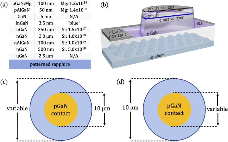
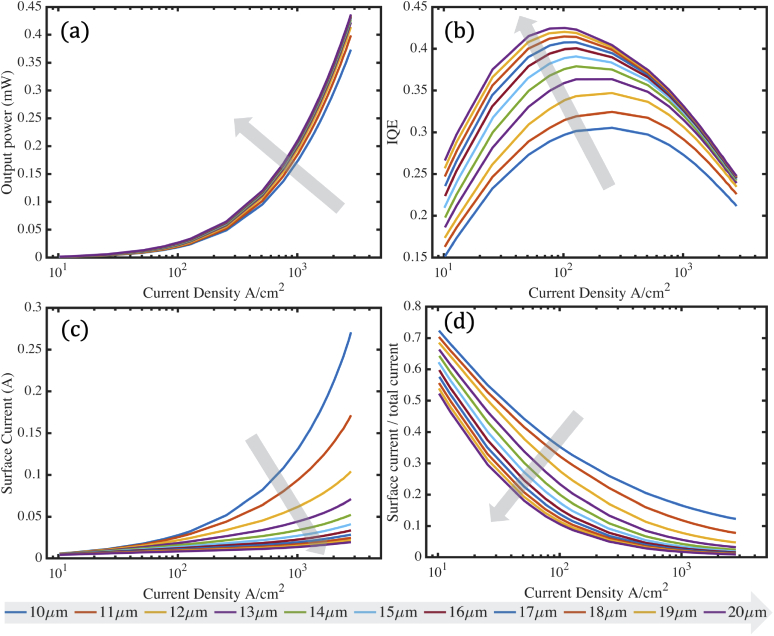
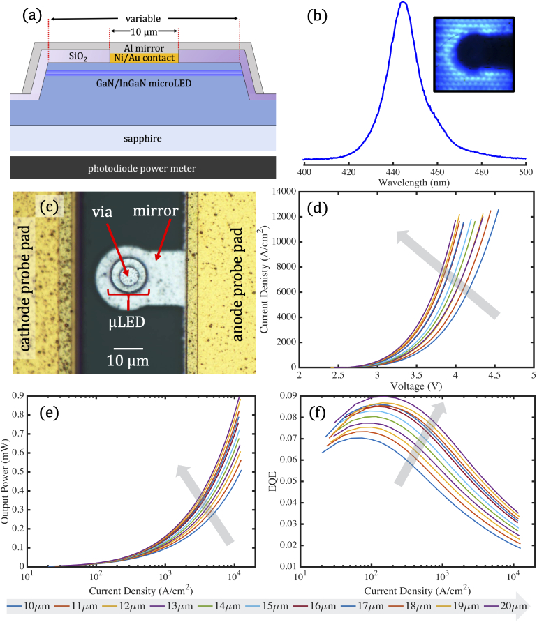
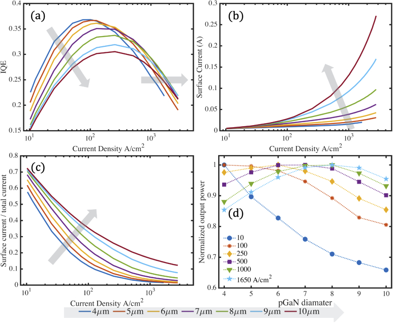
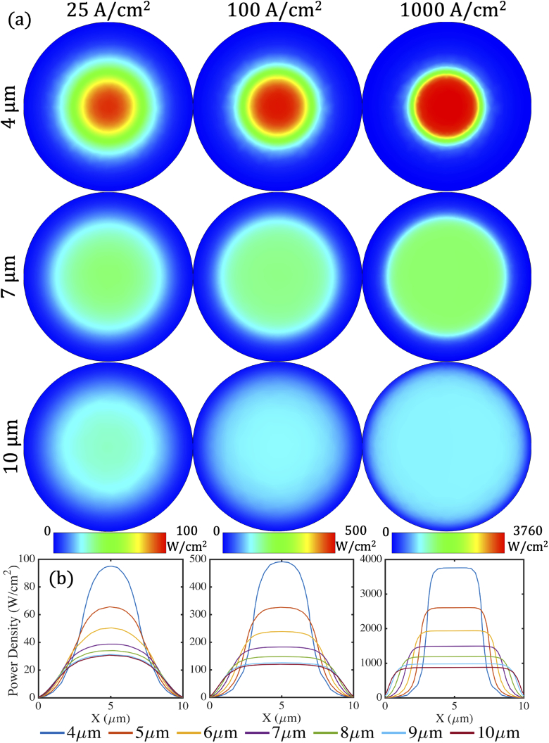
Micro light-emitting diode (microLED) structures were modeled and validated with fabricated devices to investigate p-type GaN (pGaN) contact size dependence on power output efficiency. Two schemes were investigated: a constant 10 μm diameter pGaN contact and varying microLED sizes and a constant 10 μm diameter microLED with varying contact sizes. Modeled devices show a 17% improvement in output power by increasing the microLED die size. Fabricated devices followed the same trend with a 70% improvement in power output. Modeled microLED devices of a constant size and varying inner contact sizes show optimized power output at different current densities for various contact sizes. In particular, lower current densities show optimized output for smaller pGaN contacts and trend towards larger contacts for higher current densities in a balance between undesirable efficiency losses at high-current injection and preventing surface recombination losses. We show that for all device geometries, it is preferential to shrink the pGaN contact to maximize efficiency by suppressing surface recombination losses and further improvements should be carefully considered to optimize efficiency for a desired operational brightness.
Conflict of interest statement
The authors declare no conflicts of interest.
Figures
Similar articles
-
Effects of ITO Contact Sizes on Performance of Blue Light MicroLEDs.Nanoscale Res Lett. 2022 Nov 28;17(1):113. doi: 10.1186/s11671-022-03754-9. Nanoscale Res Lett. 2022. PMID: 36437416 Free PMC article.
-
3200 ppi Matrix-Addressable Blue MicroLED Display.Micromachines (Basel). 2022 Aug 19;13(8):1350. doi: 10.3390/mi13081350. Micromachines (Basel). 2022. PMID: 36014272 Free PMC article.
-
Monolithic integrated all-GaN-based µLED display by selective area regrowth.Opt Express. 2023 Sep 11;31(19):31300-31307. doi: 10.1364/OE.502275. Opt Express. 2023. PMID: 37710652
-
Nitride micro-LEDs and beyond--a decade progress review.Opt Express. 2013 May 6;21 Suppl 3:A475-84. doi: 10.1364/OE.21.00A475. Opt Express. 2013. PMID: 24104436
-
Implantable Micro-Light-Emitting Diode (µLED)-based optogenetic interfaces toward human applications.Adv Drug Deliv Rev. 2022 Aug;187:114399. doi: 10.1016/j.addr.2022.114399. Epub 2022 Jun 15. Adv Drug Deliv Rev. 2022. PMID: 35716898 Review.
Cited by
-
MicroLED/LED electro-optical integration techniques for non-display applications.Appl Phys Rev. 2023 Jun;10(2):021306. doi: 10.1063/5.0125103. Appl Phys Rev. 2023. PMID: 37265477 Free PMC article. Review.
-
Advanced technologies in InGaN micro-LED fabrication to mitigate the sidewall effect.Light Sci Appl. 2025 Jan 26;14(1):64. doi: 10.1038/s41377-025-01751-y. Light Sci Appl. 2025. PMID: 39863583 Free PMC article. Review.
-
Investigation of Enhanced Ambient Contrast Ratio in Novel Micro/Mini-LED Displays.Nanomaterials (Basel). 2021 Dec 6;11(12):3304. doi: 10.3390/nano11123304. Nanomaterials (Basel). 2021. PMID: 34947653 Free PMC article.
-
MicroLED light source for optical sectioning structured illumination microscopy.Opt Express. 2023 May 8;31(10):16709-16718. doi: 10.1364/OE.486754. Opt Express. 2023. PMID: 37157744 Free PMC article.
References
-
- Zhou X., Tian P., Sher C.-W., Wu J., Liu H., Liu R., Kuo H.-C., “Growth, transfer printing and colour conversion techniques towards full-colour micro-LED display,” Prog. Quantum Electron. 71, 100263 (2020).10.1016/j.pquantelec.2020.100263 - DOI
-
- Olivier F., Tirano S., Dupré L., Aventurier B., Largeron C., Templier F., “Influence of size-reduction on the performances of GaN-based micro-LEDs for display application,” J. Lumin. 191, 112–116 (2017).10.1016/j.jlumin.2016.09.052 - DOI
Grants and funding
LinkOut - more resources
Full Text Sources
Other Literature Sources