Review
. 2021 Apr 28:15:661667.
doi: 10.3389/fnins.2021.661667. eCollection 2021.

Multi-Level Neuromorphic Devices Built on Emerging Ferroic Materials: A Review

Affiliations
Review

Multi-Level Neuromorphic Devices Built on Emerging Ferroic Materials: A Review

Cheng Wang et al. Front Neurosci. .

Abstract

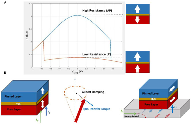
Achieving multi-level devices is crucial to efficiently emulate key bio-plausible functionalities such as synaptic plasticity and neuronal activity, and has become an important aspect of neuromorphic hardware development. In this review article, we focus on various ferromagnetic (FM) and ferroelectric (FE) devices capable of representing multiple states, and discuss the usage of such multi-level devices for implementing neuromorphic functionalities. We will elaborate that the analog-like resistive states in ferromagnetic or ferroelectric thin films are due to the non-coherent multi-domain switching dynamics, which is fundamentally different from most memristive materials involving electroforming processes or significant ion motion. Both device fundamentals related to the mechanism of introducing multilevel states and exemplary implementations of neural functionalities built on various device structures are highlighted. In light of the non-destructive nature and the relatively simple physical process of multi-domain switching, we envision that ferroic-based multi-state devices provide an alternative pathway toward energy efficient implementation of neuro-inspired computing hardware with potential advantages of high endurance and controllability.

Keywords: computing; device; ferroelectric; multi-level; neuromorphic; spintronic.


Conflict of interest statement

The authors declare that the research was conducted in the absence of any commercial or financial relationships that could be construed as a potential conflict of interest.

Figures

Figure 1
Figure 1
Concept of a biological neural network and its hardware implementation in crossbar arrays. Left panel illustrates that two biological neurons are interconnected by a synapse. The strength of the synaptic connections (synaptic weights) can be modified depending on the relationship between the two neurons. A crossbar array implementing artificial neural networks containing neurons connected by synaptic devices is shown in the right panel. The center panel describes synapse (top) and neuron (bottom) models. The activation of a neuron is controlled by its membrane potential, and its dynamics can be described of a leaky integrate-fire (LIF) neuron model. An accurate description of the membrane potential desires devices that can represent analog state values. Neurons are interconnected by synapses, which can be put into crossbar devices with variable conductance states. Spiking timing dependence plasticity (STDP) and pulse driven potentiation/depression of a synapse is shown to illustrate one bio-plausible learning mechanism based on synaptic plasticity.
Figure 2
Figure 2
(A) Magnetic tunnel junction (MTJ) and tunneling magnetoresistance (TMR). Resistance of MTJ depends on the relative orientations of the two ferromagnetic layers next to the tunnel barrier. High/low resistance states correspond to anti-parallel (AP)/parallel (P) configuration of the magnetic ordering in the free layer and reference layer. (B) Spin transfer torque (STT) and spin-orbit torque (SOT). STT is originated from spin polarized current going through an MTJ. The STT effectively switches spins by countering against the Gilbert damping of the free layer magnetic moments. SOT is a result of spin Hall effect at interface of ferromagnetic/heavy metal layers, where a charge current flowing along the heavy metal layer can induce a transverse spin current flowing into the adjacent ferromagnetic layer.
Figure 3
Figure 3
Domain wall motion (DWM) based multi-level devices. (A) STT-driven DWM in a MTJ-based device. Lequeux et al. Scientific Reports 6, 31510 (2016), Copyright 2016 Author(s), licensed under a Creative Commons Attribution (CC BY) license. (B) SOT-driven DWM device. Dzyaloshinskii-Moriya exchange interaction across the heavy metal and ferromagnetic layer provides effective magnetic fields that ensure deterministic switching. Reproduced with permission from Sengupta et al. IEEE Transactions on Biomedical Circuits and Systems, 10, 1152–1160 (2016), Copyright 2016 IEEE.
Figure 4
Figure 4
(A) All-spin crossbar array with both synapse and neurons based on SOT-DWM devices. (B) DWM-based spintronic synaptic devices. (C) DWM-based analog and IF spiking neurons. Figures reproduced with permission from Sengupta and Roy, Appl. Phys. Rev. 4, 041105 (2017). Copyright 2017 AIP Publishing.
Figure 5
Figure 5
(A) Exchange-coupled F/AF bilayer structures with multi-level states. The top panel illustrates the bilayer structure and magnetic configurations, while the bottom panel shows multi-level Hall resistance and hysteresis loop. Figure adapted with permission from Borders et al. Appl. Phys. Express 10 013007 (2017). (B) Exchange-coupled continuous-granular structures with multi-level states. The top panel shows the material structure of the continuous/granular composite, while the bottom panel shows multi-state magnetization under an increasing writing field. Figure adapted with permissions from Choe et al. IEEE Trans. Mag., 41, 3172–3174 (2005) Copyright 2005 IEEE, Tham et al. IEEE Trans. Mags. 43, 671–675 (2007) Copyright 2007 IEEE, and Wang et al. U.S. Patent Application No. 16/255,698.
Figure 6
Figure 6
Neuromorphic implementation based on exchange-coupled heterostructures. (A) Modifications of synaptic weights stored in F/AF devices after training for pattern recognition. Figure reproduced with permission from Borders et al. Appl. Phys. Express 10 013007 (2017). (B) STDP demonstration based on the Hall resistance of F/AF devices. (C) Effect of input pulses on the synaptic state of F/AF devices. Figures reproduced with permission from Kurenkov et al. Advanced Materials 31, 1900636 (2019). (D) Resistance modifications of an antiferromagnetic material CuMnAs under pulses of various lengths. Figure reproduced from Olejník, K. et al. Nat. Commun. 8, 15434 (2017). Copyright 2017 Author(s), licensed under a Creative Commons Attribution (CC BY) license.
Figure 7
Figure 7
(A) Image of polycrystalline multigranular HfZrO2 thin film, where average grain size is around 30 nm. Figure reproduced with permission from Lederer et al. Appl. Phys. Lett. 115, 222902 (2019) Copyright 2019 AIP Publishing. (B) Polarization-electric field (P-E) loops with hysteresis of HfO2. Figure reproduced with permission from Zhou et al. Acta Mater. 99 (2015) 240–246. Copyright 2015 ELSEIVER. (C) Device structure of a FeFET. (D) Conductance states of FeFET modulated by the gate voltage. Figure reproduced with permission from Mulaosmanovic et al. (2017) Symposium on VLSI Technology (p. T176–T177) Copyright 2017 IEEE.
Figure 8
Figure 8
(A) Crossbar implementation of multi-level FeFET cells for neuromorphic computing. Figure reproduced with permission from Jerry et al. (2017) IEEE International Electron Devices Meeting (IEDM), p. 6-2, Copyright 2017 IEEE. (B) Ferroelectric-based device emulating a leaky-integrate-fire (LIF) neuron. Figure reproduced with permission from Dutta et al. (2019) Symposium on VLSI Technology T140-T141 (IEEE) Copyright 2019 IEEE. (C) Voltage pulsing scheme achieving synaptic weight updates in FeFET devices with improved symmetry in conductance change during potentiation and depression processes. Figure reproduced with permission from Jerry et al. In 2017 IEEE International Electron Devices Meeting (IEDM), p. 6-2, Copyright 2017 IEEE. (D) FeFET based IF spiking neuron. The firing of neuron can be observed and sensed from the abrupt change of drain current. Figure adapted from Mulaosmanovic, et al. Nanoscale 10, 21755–21763 (2018) with permission from The Royal Society of Chemistry.
Figure 9
Figure 9
(A) Multi-level state characterized by tunneling electro-resistance of a FTJ comprising BaTiO3 as the tunnel barrier sandwiched between Au/Co and LSMO electrodes. The resistance states are found to follow the percentage of domains switched by applied voltages. Figure reproduced with permission from Chanthbouala et al. Nat. Mater. 11, 860–864 (2012). Copyright 2012 Springer Nature. (B) Gradual conductance change of a BaFeO3 based FTJ under accumulated pulses is experimentally observed to be closely associated with the switching process of ferroelectric multi-domains. The behavior of conductance change under pulses can be directly implemented into neuromorphic functionalities such as synaptic plasticity. Figure reproduced from Boyn et al. Nat. Commun. 8, 14736 (2017). Copyright 2017, Authors, licensed under a Creative Commons Attribution (CC BY) license.
Figure 10
Figure 10
(A) Demonstration of synaptic potentiation and depression in a BaTiO3-based FTJ. Figure reproduced with permission from Chanthbouala et al. Nat. Mat. 11, 860–864 (2012) Copyright 2012 Springer Nature. (B) STDP demonstration in BaFeO3 based FTJ. Figure reproduced from Boyn et al. Nat. Comm. 8, 14736 (2017). Copyright 2017, Authors, licensed under a Creative Commons Attribution (CC BY) license. (C) Demonstration of synaptic potentiation and depression and (D) STDP in HfOx based FTJ. Figures reproduced with permission from Yoong et al. Adv. Funct. Mater. 2018, 28, 1806037. Copyright 2018 WILEY-VCH Verlag GmbH & Co. KGaA, Weinherm.
Figure 11
Figure 11
In-memory computing architecture involving multiple tiles of interconnected crossbar arrays to process high dimensional MVM operations with high bit precision. (A) Illustration of the multi-tile architecture for executing large input vector with high bit precision where multiple crossbars will be used for mapping the input and weight matrix. (B) Illustration of the circuit of a single crossbar array comprising the array of synaptic devices in series with access transistors and peripheral analog and digital circuits. A multiplexer (MUX) and transimpediance amplifier (TIA) are directly connected to the crossbar columns, followed by sample and hold circuit (S&H) as well as ADC and shift and add circuitry.

Similar articles

Cited by

References

    1. Adam G. C., Hoskins B. D., Prezioso M., Merrikh-Bayat F., Chakrabarti B., Strukov D. B. (2017). 3-d memristor crossbars for analog and neuromorphic computing applications. IEEE Trans. Electron Dev. 64, 312–318. 10.1109/TED.2016.2630925 - DOI
    1. Agrawal A., Roy K. (2018). Mimicking leaky-integrate-fire spiking neuron using automotion of domain walls for energy-efficient brain-inspired computing. IEEE Trans. Magn. 55, 1–7. 10.1109/TMAG.2018.2882164 - DOI
    1. Ambriz-Vargas F., Kolhatkar G., Thomas R., Nouar R., Sarkissian A., Gomez-Yá nez C., et al. . (2017). Tunneling electroresistance effect in a Pt/Hf0.5 Zr 0.5 O 2/Pt structure. Appl. Phys. Lett. 110:093106. 10.1063/1.4977028 - DOI
    1. Ambrogio S., Narayanan P., Tsai H., Shelby R. M., Boybat I., Di Nolfo C., et al. . (2018). Equivalent-accuracy accelerated neural-network training using analogue memory. Nature 558, 60–67. 10.1038/s41586-018-0180-5 - DOI - PubMed
    1. Ankit A., Hajj I. E., Chalamalasetti S. R., Ndu G., Foltin M., Williams R. S., et al. . (2019). Puma: a programmable ultra-efficient memristor-based accelerator for machine learning inference, in Proceedings of the Twenty-Fourth International Conference on Architectural Support for Programming Languages and Operating Systems (Providence, RI: ), 715–731. 10.1145/3297858.3304049 - DOI

LinkOut - more resources