. 2021 May 21;12(1):3011.
doi: 10.1038/s41467-021-23332-4.

DNA origami single crystals with Wulff shapes

Affiliations

DNA origami single crystals with Wulff shapes

Yong Wang et al. Nat Commun. .

Abstract

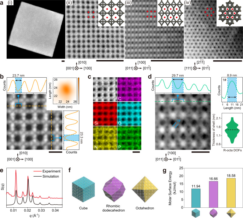
DNA origami technology has proven to be an excellent tool for precisely manipulating molecules and colloidal elements in a three-dimensional manner. However, fabrication of single crystals with well-defined facets from highly programmable, complex DNA origami units is a great challenge. Here, we report the successful fabrication of DNA origami single crystals with Wulff shapes and high yield. By regulating the symmetries and binding modes of the DNA origami building blocks, the crystalline shapes can be designed and well-controlled. The single crystals are then used to induce precise growth of an ultrathin layer of silica on the edges, resulting in mechanically reinforced silica-DNA hybrid structures that preserve the details of the single crystals without distortion. The silica-infused microcrystals can be directly observed in the dry state, which allows meticulous analysis of the crystal facets and tomographic 3D reconstruction of the single crystals by high-resolution electron microscopy.


Conflict of interest statement

The authors declare no competing interests.

Figures

Fig. 1
Fig. 1. Formation of microcrystals with Wulff shapes.
a Crystallization of cubic microcrystals (a = b = c) from R-octa DOFs through a slow annealing process. Middle scheme: DNA sequences of sticky ends in the R-octa system. Bottom right panel: representative TEM image of a bare microcrystal. b Schematic illustration of the silica-encapsulation strategy for DNA microcrystals. The process is realized through the involvement of TMAPS (red spheres) and TEOS (black spheres), see details in Methods section. c Model (left) and representative SEM image (right) of an encapsulated microcrystal with the same orientation. d Crystallization of cuboid microcrystals (a = b < c) from E-octa DOFs through a slow annealing procedure. Middle scheme: DNA sequences of sticky ends in the E-octa system. Bottom left panel: representative TEM image of a bare microcrystal. e Representative SEM image (left) and model (right) of an encapsulated microcrystal with a cuboid shape. Scale bars: 2 μm. Note that: the number of monomers drawn in the conceptual drawing in (a and d) are much less than real condition to highlight the linking mode between monomers.
Fig. 2
Fig. 2. SEM images and analysis of Wulff-shaped microcrystals.
a Left: large-scaled SEM image of cubic microcrystals. Right: size distribution of 100 microcrystals (n = 100), average edge length: 3.51 ± 0.98 μm (mean ± SD). Scale bar: 20 μm. b Large-scale SEM image of cuboid microcrystals. Middle: size distribution of 50 microcrystals (n = 50) in terms of a (blue) and c (purple), average edge length of a: 2.69 ± 0.59 μm (mean ± SD), average edge length of c: 4.69 ± 1.04 μm (mean ± SD). Right: distribution of the ratio between a (or b) and c of microcrystals. Scale bar: 10 μm. c SEM image of an individual cubic microcrystal. Top right panel: close-up view of a partial region with a vacancy inside (enclosed by the red square) and corresponding model. Surficial steps are labelled with blue and indicated in the schematic. Scale bar: 1 μm. d SEM image of an individual cuboid microcrystal. Top left panel: close-up view of a partial region with a vacancy inside (enclosed by the red square) and corresponding model. A surficial adatom is labelled with green and indicated in the schematic as well. Scale bar: 1 μm. Source data are provided as a Source Data file.
Fig. 3
Fig. 3. Determination of the structure and internal uniformity of cubic microcrystals.
a HAADF-STEM image of a free-standing cubic microcrystal (i); close-up views of multiple facets (ii–iv) obtained by observation along different orientations, with models inserted in the top right panels. Scale bars: 250 nm. b Enlarged image of an arbitrary partial region of a (ii). Top and right panels: size measurements of external pores by line profile analysis. Top right panel: size distribution of external pores. Scale bar: 50 nm. c HR-EDS mapping of the porous structure. C, Si, O, N, and P were determined and are labelled in purple, red, cyan, yellow and green, respectively. Scale bar: 50 nm. d Enlarged image of an arbitrary partial region of a (iii), with length (top) and width (top right) measurements of silicified bundles by line profile analysis, and thickness distribution of the silica shell (bottom right). Scale bar: 50 nm. e Representative one-dimensional SAXS result (red curve) and fitting (black curve) of encapsulated cubic crystals. f Schematics of different shape Wulff polyhedra exposing different facets composed of R-octa DOFs. g Comparison of molar surface energies of exposed surfaces among different Wulff shapes. Source data are provided as a Source Data file.
Fig. 4
Fig. 4. Structural analysis and reconstruction of cuboid microcrystals.
a Representative HAADF-STEM image of an individual cuboid microcrystal. Scale bar: 1 μm. b Zoomed-in view of a nanoscopic region arbitrarily selected from the crystal oriented along the [100] zone-axis. Top and right panels: size measurements of pores by line profile analysis. Top right panel: size distribution of mesopores. Scale bar: 50 nm. c HR-EDS mapping of the mesoporous configuration. C, Si, O, N, and P are coloured in purple, red, cyan, yellow and green, respectively. Scale bar: 50 nm. d Left: zoomed-in image of nanoscopic partial region observed along the [110] zone-axis. Right: length (top panel) and width (bottom panels) measurements of silicified bundles by line profile analysis. Scale bar: 50 nm. e Thickness distribution of the silica shell encapsulated on cuboid crystals. f, g 3D reconstruction of a piece of a microcrystal. The 3D rendered results are exhibited along two perpendicular axes and the cross-sectional images were extracted from the red (f) and green (g) planes along different directions. Obtained tomographic images are enclosed by corresponding coloured rectangles. Scale bars: 250 nm.

Similar articles

Cited by

References

    1. Zheng J, et al. From molecular to macroscopic via the rational design of a self-assembled 3D DNA crystal. Nature. 2009;461:74–77. doi: 10.1038/nature08274. - DOI - PMC - PubMed
    1. Auyeung E, et al. DNA-mediated nanoparticle crystallization into Wulff polyhedra. Nature. 2014;505:73–77. doi: 10.1038/nature12739. - DOI - PubMed
    1. Ross MB, Ku JC, Vaccarezza VM, Schatz GC, Mirkin CA. Nanoscale form dictates mesoscale function in plasmonic DNA-nanoparticle superlattices. Nat. Nanotechnol. 2015;10:453–458. doi: 10.1038/nnano.2015.68. - DOI - PubMed
    1. Park DJ, et al. Plasmonic photonic crystals realized through DNA-programmable assembly. Proc. Natl Acad. Sci. USA. 2015;112:977–981. doi: 10.1073/pnas.1422649112. - DOI - PMC - PubMed
    1. Zhao JM, et al. Post-assembly stabilization of rationally designed DNA crystals. Angew. Chem. Int. Ed. 2015;54:9936–9939. doi: 10.1002/anie.201503610. - DOI - PubMed

Publication types

LinkOut - more resources