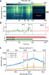
Intrinsic luminescence blinking from plasmonic nanojunctions
- PMID: 34021133
- PMCID: PMC8139969
- DOI: 10.1038/s41467-021-22679-y
Intrinsic luminescence blinking from plasmonic nanojunctions
Abstract
Plasmonic nanojunctions, consisting of adjacent metal structures with nanometre gaps, can support localised plasmon resonances that boost light matter interactions and concentrate electromagnetic fields at the nanoscale. In this regime, the optical response of the system is governed by poorly understood dynamical phenomena at the frontier between the bulk, molecular and atomic scales. Here, we report ubiquitous spectral fluctuations in the intrinsic light emission from photo-excited gold nanojunctions, which we attribute to the light-induced formation of domain boundaries and quantum-confined emitters inside the noble metal. Our data suggest that photoexcited carriers and gold adatom - molecule interactions play key roles in triggering luminescence blinking. Surprisingly, this internal restructuring of the metal has no measurable impact on the Raman signal and scattering spectrum of the plasmonic cavity. Our findings demonstrate that metal luminescence offers a valuable proxy to investigate atomic fluctuations in plasmonic cavities, complementary to other optical and electrical techniques.
Conflict of interest statement
The authors declare no competing interests.
Figures


Similar articles
-
Light Emission and Conductance Fluctuations in Electrically Driven and Plasmonically Enhanced Molecular Junctions.ACS Photonics. 2024 Jun 6;11(6):2388-2396. doi: 10.1021/acsphotonics.4c00291. eCollection 2024 Jun 19. ACS Photonics. 2024. PMID: 38911841 Free PMC article.
-
Inelastic Light Scattering in the Vicinity of a Single-Atom Quantum Point Contact in a Plasmonic Picocavity.ACS Nano. 2023 Jun 13;17(11):10172-10180. doi: 10.1021/acsnano.3c00261. Epub 2023 May 15. ACS Nano. 2023. PMID: 37183801
-
Hollow Porous Gold Nanoshells with Controlled Nanojunctions for Highly Tunable Plasmon Resonances and Intense Field Enhancements for Surface-Enhanced Raman Scattering.ACS Appl Mater Interfaces. 2019 Nov 27;11(47):44458-44465. doi: 10.1021/acsami.9b16983. Epub 2019 Nov 13. ACS Appl Mater Interfaces. 2019. PMID: 31718128
-
Manipulating Light-Matter Interactions in Plasmonic Nanoparticle Lattices.Acc Chem Res. 2019 Nov 19;52(11):2997-3007. doi: 10.1021/acs.accounts.9b00345. Epub 2019 Oct 9. Acc Chem Res. 2019. PMID: 31596570
-
Advanced plasmonic technologies for multi-scale biomedical imaging.Chem Soc Rev. 2022 Nov 28;51(23):9445-9468. doi: 10.1039/d2cs00525e. Chem Soc Rev. 2022. PMID: 36378240 Review.
Cited by
-
Fluorescence engineering in metamaterial-assisted super-resolution localization microscope.Nanophotonics. 2023 Mar 31;12(13):2491-2498. doi: 10.1515/nanoph-2022-0751. eCollection 2023 Jun. Nanophotonics. 2023. PMID: 39633765 Free PMC article.
-
Plasmonic phenomena in molecular junctions: principles and applications.Nat Rev Chem. 2022 Oct;6(10):681-704. doi: 10.1038/s41570-022-00423-4. Epub 2022 Sep 20. Nat Rev Chem. 2022. PMID: 37117494 Review.
-
Nanoparticle-on-mirror pairs: building blocks for remote spectroscopies.Nanophotonics. 2022 Oct 27;11(22):5153-5163. doi: 10.1515/nanoph-2022-0521. eCollection 2022 Dec. Nanophotonics. 2022. PMID: 39634305 Free PMC article.
-
In-operando control of sum-frequency generation in tip-enhanced nanocavities.Light Sci Appl. 2025 May 22;14(1):203. doi: 10.1038/s41377-025-01855-5. Light Sci Appl. 2025. PMID: 40404638 Free PMC article.
-
Quantum Plasmonics in Sub-Atom-Thick Optical Slots.Nano Lett. 2023 Dec 13;23(23):10696-10702. doi: 10.1021/acs.nanolett.3c02537. Epub 2023 Nov 29. Nano Lett. 2023. PMID: 38029409 Free PMC article.
References
-
- Xu H, Bjerneld EJ, Käll M, Börjesson L. Spectroscopy of single hemoglobin molecules by surface enhanced Raman scattering. Phys. Rev. Lett. 1999;83:4357–4360. doi: 10.1103/PhysRevLett.83.4357. - DOI
Grants and funding
- 820196/EC | Horizon 2020 Framework Programme (EU Framework Programme for Research and Innovation H2020)
- 820196/EC | Horizon 2020 Framework Programme (EU Framework Programme for Research and Innovation H2020)
- 820196/EC | EU Framework Programme for Research and Innovation H2020 | H2020 Priority Excellent Science | H2020 European Research Council (H2020 Excellent Science - European Research Council)
- 820196/EC | EU Framework Programme for Research and Innovation H2020 | H2020 Priority Excellent Science | H2020 European Research Council (H2020 Excellent Science - European Research Council)
- 820196/EC | EU Framework Programme for Research and Innovation H2020 | H2020 Priority Excellent Science | H2020 European Research Council (H2020 Excellent Science - European Research Council)
LinkOut - more resources
Full Text Sources
Other Literature Sources

