Review
. 2021 Jul;8(14):e2100569.
doi: 10.1002/advs.202100569. Epub 2021 May 24.

Recent Progress on Electrical and Optical Manipulations of Perovskite Photodetectors

Affiliations
Review

Recent Progress on Electrical and Optical Manipulations of Perovskite Photodetectors

Fang Wang et al. Adv Sci (Weinh). 2021 Jul.

Abstract

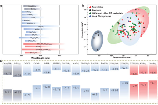
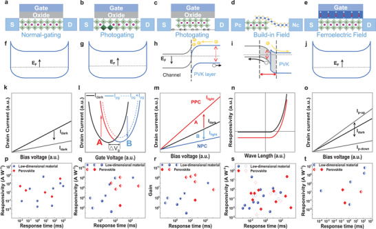
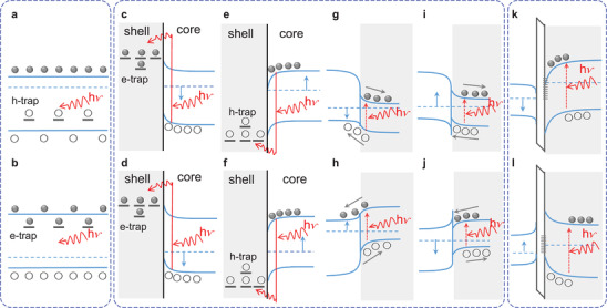
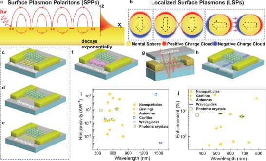
Photodetectors built from conventional bulk materials such as silicon, III-V or II-VI compound semiconductors are one of the most ubiquitous types of technology in use today. The past decade has witnessed a dramatic increase in interest in emerging photodetectors based on perovskite materials driven by the growing demands for uncooled, low-cost, lightweight, and even flexible photodetection technology. Though perovskite has good electrical and optical properties, perovskite-based photodetectors always suffer from nonideal quantum efficiency and high-power consumption. Joint manipulation of electrons and photons in perovskite photodetectors is a promising strategy to improve detection efficiency. In this review, electrical and optical characteristics of typical types of perovskite photodetectors are first summarized. Electrical manipulations of electrons in perovskite photodetectors are discussed. Then, artificial photonic nanostructures for photon manipulations are detailed to improve light absorption efficiency. By reviewing the manipulation of electrons and photons in perovskite photodetectors, this review aims to provide strategies to achieve high-performance photodetectors.

Keywords: electric manipulations; optical manipulations; perovskite photodetectors.


Conflict of interest statement

The authors declare no conflict of interest.

Figures

Figure 1
Figure 1
a) Detection ranges for different perovskite photodetectors. b) Comparison of the performances of photodetectors based on perovskite and low‐dimensional materials. c) Band structures for some common perovskite materials.
Figure 2
Figure 2
Perovskite photodetectors of different electric manipulations. a–e) Device structures of perovskite photodetectors with gate voltage field, photogating effect, built in electric field, and ferroelectric field manipulations. f–j) Schematic diagram of band structure for perovskite photodetectors with gate voltage field, photogating effect, built in electric field, and ferroelectric field manipulations. k–o) Typical characteristic curves for perovskite photodetectors with gate voltage field, photogating effect, built in electric field, and ferroelectric field manipulations. p–t) Performance for perovskite photodetectors compared with traditional low‐dimensional photodetectors manipulated by gate voltage field, photogating effect, built in electric field, and ferroelectric field. The red diamonds refer to perovskite photodetectors, the blue circles refer to 2D photodetectors, and the blue stars refer to nanowire photodetectors. The solid points represent manipulation mechanism within single materials, the half‐solid points represent manipulation mechanism of hybrid structures, and the hollow points represent manipulation mechanism of Schottky junction.
Figure 3
Figure 3
Photogating mechanism in three types of structures. The shaded part represents the gating layer. a,b) Photogating mechanism occurring in a single material with hole‐ or electron‐trap center. c–f) Photogating mechanism based on core–shell structure with a gating layer of insulator. The electron‐traps in the gating layer decrease the Fermi level and result in a negative response for n‐type semiconductor or a positive response for a p‐type semiconductor. The hole‐traps in the gating layer increase the Fermi level and result in a positive response for n‐type semiconductor or a negative response for a p‐type semiconductor. g,h) Photogating mechanism based on type II heterojunction. The photoinduced carriers transfer into the channel and change the response of the perovskite. i,j) Photogating mechanism based on type I heterojunction. The trapped carriers at the interface could result in a positive or negative response of the photodetector. k,l) Photogating mechanism in hybrid structure of three materials. Here, the photoinduced carriers are blocked by the infinite high barrier and trapped at the interface. The trap‐state will act as a gating role to manipulate the conduction characteristic of the channel.
Figure 4
Figure 4
Perovskite photodetectors with different optical manipulations. a) SPP caused by the interaction of free electrons and photons propagating at the interface between the metal structure and perovskite. b) Localized electromagnetic oscillation of the LSP in the seal surface of the microstructures without propagation. c–e) Typical optical manipulation structures of nanoparticles, gratings, and antennas for perovskite photodetectors based on SPP and LSP. f) Optical manipulation structure of photonic crystal. g) Optical manipulation structure of photonic crystal. h) Typical optical manipulation structure of waveguide. i,j) Responsivity and enhancement of the published perovskite photodetectors with different optical enhancement. Here, the yellow point refers to performance of perovskite photodetectors based on the nanoparticle, the yellow square refers to the manipulation of grating, and the yellow triangle refers to the antenna. The hollow pentagon represents the perovskite photodetectors with photonic crystals. The hollow square represents the manipulation of resonant cavities. The stick represents waveguides. The overlapped points in the graph indicate the multiple optical manipulation mechanisms within one perovskite photodetector.

References

    1. Rose A., Concepts in Photoconductivity and Allied Problems, Interscience Publishers, New York: 1963.
    1. Bube R. H., Photoelectronic Properties of Semiconductors, Cambridge University Press, Cambridge: 1992.
    1. Saleh B., Teich M., Fundamentals of Photonics, John Wiley & Sons, Hoboken, NJ: 2019.
    1. Konstantatos G., Sargent E., Nat. Nanotechnol. 2010, 5, 391. - PubMed
    1. Fridkin V., Crystallogr. Rep. 2001, 46, 654.

LinkOut - more resources