Review
. 2021 May 25;16(1):94.
doi: 10.1186/s11671-021-03551-w.

2D Semiconductor Nanomaterials and Heterostructures: Controlled Synthesis and Functional Applications

Affiliations
Review

2D Semiconductor Nanomaterials and Heterostructures: Controlled Synthesis and Functional Applications

Hongyan Xu et al. Nanoscale Res Lett. .

Abstract

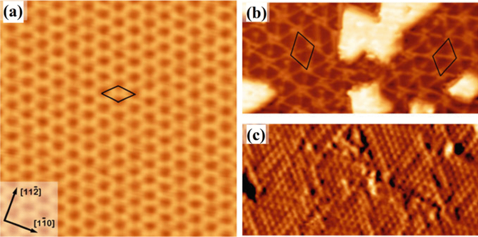
Two-dimensional (2D) semiconductors beyond graphene represent the thinnest stable known nanomaterials. Rapid growth of their family and applications during the last decade of the twenty-first century have brought unprecedented opportunities to the advanced nano- and opto-electronic technologies. In this article, we review the latest progress in findings on the developed 2D nanomaterials. Advanced synthesis techniques of these 2D nanomaterials and heterostructures were summarized and their novel applications were discussed. The fabrication techniques include the state-of-the-art developments of the vapor-phase-based deposition methods and novel van der Waals (vdW) exfoliation approaches for fabrication both amorphous and crystalline 2D nanomaterials with a particular focus on the chemical vapor deposition (CVD), atomic layer deposition (ALD) of 2D semiconductors and their heterostructures as well as on vdW exfoliation of 2D surface oxide films of liquid metals.

Keywords: 2D semiconductors; Atomic layer deposition; Heterostructures; Synthesis.


Conflict of interest statement

The authors declare that they have no competing interests.

Figures

Fig. 1
Fig. 1
Dynamics of number of published articles for “2D semiconductors” based on Web of Knowledge™
Fig. 2
Fig. 2
Properties of 2D semiconductors utilized in their typical applications
Fig. 3
Fig. 3
STM image of a the honeycomb Ti2O3 structure, and b pinwheel TiO monolayer grown on Au (111), and c atomically resolved STM image of pinwheel structures on Au (111). Reproduced with permission from [83]
Fig. 4
Fig. 4
Wafer-scale MOCVD growth of continues MoS2 and WS2 film. a The graphical schematic of CVD device and the related precursors for MOCVD of 2D MoS2 and WS2 films. c The batch of 8100 FET devices based on 2D MoS2 film over Si/SiO2 wafer. The inset shows the enlarged image of one mm square containing 100 devices. d The sequential fabrication stage of stacked MoS2-based device. e The image demonstrates the MoS2 FET devices on first and second layers. f The IDS-VDS of two neighboring FET devices on two different layers. Reprinted with permission from [88]
Fig. 5
Fig. 5
a Schematic of CVD growth of semiconductor/semiconductor lateral 2D heterostructures. b Atomic resolution contrast STEM images of in-plane interface between WS2 and MoS2. c The Raman intensity mapping of 2D heterostructured 2D film at 351 cm−1 (yellow) and 381 cm−1 (purple). d The combined PL intensity mapping at 630 nm (orange) and 680 nm (green). Reprinted and reproduced with permission from [89]
Fig. 6
Fig. 6
Number of annual citations on “Atomic layer deposition” topic a of published manuscripts. Data are according to Web of Knowledge™ Database. Comparison of the deposition rate vs step coverage (b) and coverage areas produced by different deposition techniques (c). Comparative analysis of properties of SE fabricated by PVD, CVD, and ALD, respectively (d). Reproduced with permission from [94]
Fig. 7
Fig. 7
a Cross-sectional image from the interface between ALD grown Sb2Te3 on graphene/SiO2 substrate. b The cross-sectional image of heterostructured Sb2Te3/Bi2Te3 stacked layers. c The HRTEM image of SnS/WS2 heterointerfaces and d the corresponding fast Fourier transform (FFT) image. Reproduced with permission from [138]
Fig. 8
Fig. 8
a Graphical scheme of deposition of 2D MoO3 nanofilms by PE-ALD. b The injection of precursor into ALD chamber and c the reaction between precursor and Au surface (d) and the complete deposition of a monolayer film over Au substrate. e The thickness of PE-ALD MoO3 film over Au substrate vs. the ALD cycle number at based on the usage of (NtBu)2(NMe2)2Mo precursor and O2 plasma at 150 °C and 250 °C, with the precursor dosing time of 2 s and plasma exposure time of 5 s. f The saturation curve of (NtBu)2(NMe2)2Mo precursor. The GPC is demonstrated as the function of precursor dosing time. g The saturation curve for O2 plasma showing the GPC as the function of plasma exposure time. Reproduced with permission from [141]
Fig. 9
Fig. 9
Enhancement of non-stoichiometry in monolayer WO3 film developed by ALD via intercalation/de-intercalation process
Fig. 10
Fig. 10
a Graphical representation of vdW exfoliation method. When a Si/SiO2 substrate is attached to the molten tin alloy, the created vdW force between the tin oxide and SiO2 surface help to delamination and following attachment of 2D oxide film to the SiO2 substrate. b The AFM image of the monolayer (0.6 nm) and bilayer (1.2 nm) tin oxide film. c The TEM image of tin oxide film developed in controlled atmosphere. d The HRTEM of tin oxide film developed in ambient atmosphere with mixed SnO and SnO2 structure. e The HRTEM image of SnO film developed in controlled atmosphere. f The bandgap of monolayer SnO film measured by electron energy loss spectroscopy. g The I-V characteristics of fabricated SnO FET device at various gate voltages. Reprinted with permission from [156]
Fig. 11
Fig. 11
a The side view of GaPO4 demonstrating the out-of-plane structure of GaPO4. b For the secondary phosphatization treatment. c The AFM and HRTEM studies of 2D GaPO4 film. d The XRD, e Raman and f bandgap measurement of 2D GaPO4 film. Reprinted with permission from [160]
Fig. 12
Fig. 12
a Schematic illustration of squeezing of liquid metal galinstan between SiO2 substrate and b following post-ammonolysis treatment for phase transform of Ga2O3 to GaN film. c The High resolution AFM image of the surface of GaN film. d The HRTEM image of GaN film and e the band gap of measurement of GaN film. Reprinted with permission from [160]
Fig. 13
Fig. 13
a Schematic illustration of fabrication of 2D vdW heterostructured SnO/In2O3 film. b The HRTEM image of heterostructured SnO/In2O3 films. c The HRTEM image of atomic structure of heterostructured films show the high crystalline structure of SnO and In2O3 film with their lattice spacing distance. d The AFM of heterostructured SnO/In2O3 film with e the profile thickness of the films. f The Raman spectra of SnO, In2O3 and SnO/ In2O3 2D films. g The optical absorption of SnO, In2O3 and SnO/ In2O3 2D films. h The band alignment of SnO/ In2O3 2D heterostructures. Reprinted with permission from [167]
Fig. 14
Fig. 14
a Schematic interpretation of metal/insulator/metal atomristor device based on TMDCs monolayers, b the corresponding optical image of device and the c cross-sectional TEM image of Au-Monolayer MoS2-Au device. d The atomically resolved STM image of monolayer MoS2 film deposited on Au electrode. The sulfur vacancies indicated by dashed lines. e The typical I-V curve of atomristor device based on monolayer MoS2 monolayer device. The typical bipolar RS behavior is observed. f The occasional unipolar RE behavior of device in monolayer MoS2 device. g, h and i graphs respectively demonstrate the typical bipolar RS behavior of atomristor devices based on monolayer MoSe2, WS2 and WSe2 films. Reprinted with permission from [172]
Fig. 15
Fig. 15
The optical image of Cu/MoS2 double layer/Au memristor device with scale bar of 100 μm accompanied by the graphical scheme of device with top Cu electrode and bottom Au electrode. The memristor’s crossbar area is 2 × 2 μm2. b The I-V curve of memristor device with bipolar RS with the 0.25 V Set voltage and − 0.15 V Reset voltage. e The logarithmic scale IV curve of device for the pristine state before and after forming process, and for LRS and HRS after the forming process. Reprinted with permission from [173]
Fig. 16
Fig. 16
a Typical logarithmic scale depiction of I–V sweeping graph of Pt/In-doped TiO2/Au memristor. b Device is set off, the metallic cations are distributed in top layer of In-doped TiO2 film. c The formation of filamentary conductive channels, the device is set On (Set, stage 1). d The depletion of metallic cations adjacent to the bottom electrode. The device is set off again (Reset, stage 2). e By imposing the reverse gate voltage, the metallic cations again move toward the cathode electrode (top Pt electrode) and again form a metallic cation bridge and the device is set On (Set-stage 3). f By depletion of metallic cations, at Pt electrode the device is set off again (Reset, stage 4). Reprinted with permission form [174]
Fig. 17
Fig. 17
The Pt/TiO2/Ti/Pt stacked crossbar cells: a the SEM top view of (60 nm)2 cross-point, b The TEM cross-sectional image of 100 nm2 Pt/TiO2/Ti/Pt device with c its corresponding schematic graph of the plug and disc region in the TiO2 layer. Reprinted with permission from [174]
Fig. 18
Fig. 18
Graphical scheme of triple modulated architecture of artificial 2D MoS2 synaptic device. b The analogue circuit depicting the interplay between the various parameters for stimulation of synaptic plasticity. c The interplay between the Hebbian and synaptic plasticity in MoS2-based 2D synaptic device, which depicts the enhancement in the strength of long-term potentiation functionalities of device as he function of training by electronic-mode, d Ionotronic mode and e photovoltaic mode. In photovoltaic mode, the light intensity is altered (from 0.5 to 5.25 mW mm−2) to enable training by optical pulses. Reprinted and reproduced with permission from [178]
Fig. 19
Fig. 19
The optical synaptic characteristics of In-doped ultra-thin TiO2 films. a The logarithmic scale I–V curves of ITO/In-doped/Au synaptic device. Variation of the set voltage and conductance vs changes of light intensity for pulsed lasers. c The EPSC of synaptic device induced by 7 μW cm−2 laser pulse. d The PPF of device. e The variation of PPF index vs. the pulse intervals. Inset shows the variation of energy consumption vs. pulse duration. f The variation of EPSC of synaptic device stimulated with the pulsed light with different pulse intervals. Reprinted with permission from [174]
Fig. 20
Fig. 20
Scheme of human eye receptor and nociceptor system. a The human brain as decision making unit receives the informative signals from b human eye and its sensory components including the c light receptors and nociceptors in Retina section. d Shows a typical nociceptor with its components. e Is the typical schematic representation of a natural synapse and f its artificial counterparts in conductor/ semiconductor /conductor sandwiched configuration. Reprinted with permission from [52]
Fig. 21
Fig. 21
a The photoinduced nociceptive behavior of Ga2O3 (N2)/TiO2-based heterostructured devices. The effect of light intensity (λ = 655 nm) on threshold time (t0) and saturation time (ts) of Ga2O3 (N2)/TiO2 nociceptor. The light frequency was 20 Hz. b The relaxation characteristics of Au- Ga2O3 (N2)/TiO2-ITO nociceptor. The light frequency was 20 Hz. c The distinction of photoresponse behavior of Au-Ga2O3 (N2)/TiO2-ITO nociceptor in normal and abnormal state. The light frequency was 20 Hz. d The allodynia and hyperalgesia behavior of Au-Ga2O3 (N2)/TiO2-ITO opto-nociceptor. Reprinted with permission from [179]

References

    1. Velick M, Toth PS. From two-dimensional materials to their heterostructures: An electrochemist’s perspective. Appl Mater Today. 2017;8:68–103. doi: 10.1016/j.apmt.2017.05.003. - DOI
    1. Frantzeskakis E, Rödel TC, Fortuna F, Santander-Syro AF. 2D surprises at the surface of 3D materials: Confined electron systems in transition metal oxides. J Electron Spectrosc. 2017;219:16–28. doi: 10.1016/j.elspec.2016.10.001. - DOI
    1. Castellanos-Gomez A. Why all the fuss about 2D semiconductors? Nat Photon. 2016;10:202–204. doi: 10.1038/nphoton.2016.53. - DOI
    1. Akinwandeh D, Huyghebaert C, Wang CH, et al. Graphene and two-dimensional materials for silicon technology. Nature. 2019;573:507–518. doi: 10.1038/s41586-019-1573-9. - DOI - PubMed
    1. Geim AK, Novoselov KS. The rise of graphene. Nat Mater. 2007;6:183–191. doi: 10.1038/nmat1849. - DOI - PubMed

LinkOut - more resources