Fabrication of Graphoepitaxial Gate-All-Around Si Circuitry Patterned Nanowire Arrays Using Block Copolymer Assisted Hard Mask Approach
- PMID: 34042425
- PMCID: PMC8291765
- DOI: 10.1021/acsnano.0c09232
Fabrication of Graphoepitaxial Gate-All-Around Si Circuitry Patterned Nanowire Arrays Using Block Copolymer Assisted Hard Mask Approach
Abstract
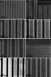
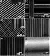
We demonstrate the fabrication of sub-20 nm gate-all-around silicon (Si) nanowire field effect transistor structures using self-assembly. To create nanopatterned Si feature arrays, a block-copolymer-assisted hard mask approach was utilized using a topographically patterned substrate with well-defined Si3N4 features for graphoepitaxially alignment of the self-assembled patterns. Microphase-separated long-range ordered polystyrene-b-poly(ethylene oxide) (PS-b-PEO) block-copolymer-derived dot and line nanopatterns were achieved by a thermo-solvent approach within the substrate topographically defined channels of various widths and lengths. Solvent annealing parameters (temperature, annealing time, etc.) were varied to achieve the desired patterns. The BCP structures were modified by anhydrous ethanol to facilitate insertion of iron oxide features within the graphoepitaxial trenches that maintained the parent BCP arrangements. Vertical and horizontal ordered Si nanowire structures within trenches were fabricated using the iron oxide features as hard masks in an inductively coupled plasma (ICP) etch process. Cross-sectional micrographs depict wires of persistent width and flat sidewalls indicating the effectiveness of the mask. The aspect ratios could be varied by varying etch times. The sharp boundaries between the transistor components was also examined through the elemental mapping.
Keywords: block copolymer; gate-all-around; graphoepitaxy; hard mask; nanowire.
Conflict of interest statement
The authors declare no competing financial interest.
Figures


References
-
- Seto J. Y. W.; Levinson Physical Modeling for Fluctuation of Grain-Boundary Resistance in Polycrystalline Silicon. The Jpn. Soc. Appl. Phys. 2018, 12158.
-
- Pantisano L.; Afanas’ev V.; Pourtois G.; Chen P. J. Valence-Band Electron-Tunneling Measurement of the Gate Work Function: Application to the High- κ /Polycrystalline-Silicon Interface. J. Appl. Phys. 2005, 98, 053712.10.1063/1.2031947. - DOI
-
- Colinge J. P.; Kranti A.; Yan R.; Lee C. W.; Ferain I.; Yu R.; Akhavan N. D.; Razavi P. Junctionless Nanowire Transistor (JNT): Properties and Design Guidelines. Solid-State Electron. 2011, 65, 33–37. 10.1016/j.sse.2011.06.004. - DOI
-
- Neisser M.; Wurm S. ITRS Lithography Roadmap: 2015 Challenges. Adv. Opt. Technol. 2015, 4, 235.10.1515/aot-2015-0036. - DOI
-
- Chen Y.; Cheng Q.; Kang W. Technological Merits, Process Complexity, and Cost Analysis of Self-Aligned Multiple Patterning. Proc. SPIE 2012, 8326, 832620.10.1117/12.916490. - DOI
LinkOut - more resources
Full Text Sources
Other Literature Sources

