. 2021 May 27;12(1):3193.
doi: 10.1038/s41467-021-23262-1.

Quantized spin Hall conductance in a magnetically doped two dimensional topological insulator

Affiliations

Quantized spin Hall conductance in a magnetically doped two dimensional topological insulator

Saquib Shamim et al. Nat Commun. .

Abstract

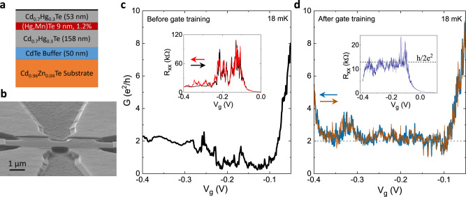
Soon after the discovery of the quantum spin Hall effect, it has been predicted that a magnetic impurity in the presence of strong Coulomb interactions will destroy the quantum spin Hall effect. However, the fate of the quantum spin Hall effect in the presence of magnetic impurities has not yet been experimentally investigated. Here, we report the successful experimental demonstration of a quantized spin Hall resistance in HgTe quantum wells dilutely alloyed with magnetic Mn atoms. These quantum wells exhibit an inverted band structure that is very similar to that of the undoped material. Micron sized devices of (Hg,Mn)Te quantum well (in the topological phase) show a quantized spin Hall resistance of h/2e2 at low temperatures and zero magnetic field. At finite temperatures, we observe signatures of the Kondo effect due to interaction between the helical edge channels and magnetic impurities. Our work lays the foundation for future investigations of magnetically doped quantum spin Hall materials towards the realization of chiral Majorana fermions.


Conflict of interest statement

The authors declare no competing interests.

Figures

Fig. 1
Fig. 1. Band structures calculated with the kp method.
a Dispersion for an infinite (Hg,Mn)Te quantum well, 9 nm thick and with 1.2% Mn, along the axis (kx,ky)=k(cos45,sin45)=k(1/2,1/2). The colors indicate the orbital character, see legend. b Three-dimensional rendering of the band structure. We highlight the axis of part a, (red curve) and the camel back points (stars). c Dispersion in the strip geometry, 500 nm wide. The colors indicate the eigenstate location 〈y〉, see legend. d Density of carriers dn/dE for the strip geometry. Just below the camel back (E ≈ −46 meV, dashed lines), the density reaches values > 400 × 105 cm−1 meV−1, out of scale in this plot.
Fig. 2
Fig. 2. Quantized spin Hall conductance in a (Hg,Mn)Te quantum well.
a Schematic of the layer stack showing the (Hg,Mn)Te quantum well sandwiched between two Cd0.7Hg0.3Te barriers on a Cd0.96Zn0.04Te substrate. b Scanning electron micrograph of a typical Hall bar used for measurements. c The conductance G as a function of gate voltage Vg for a 9 nm thick (Hg,Mn)Te quantum well with 1.2% Mn at 18 mK. The inset shows the longitudinal resistance Rxx as a function of Vg. d G as a function of Vg at 18 mK after gate training. The inset shows Rxx as a function of Vg. The dotted line indicates the expected conductance of 2e2/h in the quantum spin Hall regime. The arrows in c and d show the direction of gate voltage sweeps.
Fig. 3
Fig. 3. Effect of temperature on the quantized conductance.
a The conductance G as a function of gate voltage Vg at different temperatures from 18 mK to 4.2 K. The dotted line indicates the expected conductance of 2e2/h in the quantum spin Hall regime. b Magnified view of G as a function Vg for different temperatures to show the reproducibility in conductance fluctuations. c The average conductance in the quantum spin Hall regime Ggapav as a function of temperature T. The blue points are the experimental data and the red dashed line shows the power-law Kondo fit (see main text). The gray dashed line shows the expected thermally activated conductance [exp(Eg/2kBT)] for a band gap of Eg = 10 meV (from the band structure calculations shown in Fig. 1). The inset shows a typical GVg dependence from which Ggapav (shown by dashed horizontal line) is calculated by averaging over the conductance values in the plateau region between the dashed vertical lines.

References

    1. Kane CL, Mele EJ. Z2 topological order and the quantum spin Hall effect. Phys. Rev. Lett. 2005;95:146802. doi: 10.1103/PhysRevLett.95.146802. - DOI - PubMed
    1. Bernevig BA, Hughes TL, Zhang S-C. Quantum spin Hall effect and topological phase transition in HgTe quantum wells. Science. 2006;314:1757–1761. doi: 10.1126/science.1133734. - DOI - PubMed
    1. König M, et al. Quantum spin Hall insulator state in HgTe quantum wells. Science. 2007;318:766–770. doi: 10.1126/science.1148047. - DOI - PubMed
    1. Wu C, Bernevig BA, Zhang S-C. Helical liquid and the edge of quantum spin Hall systems. Phys. Rev. Lett. 2006;96:106401. doi: 10.1103/PhysRevLett.96.106401. - DOI - PubMed
    1. Xu C, Moore JE. Stability of the quantum spin Hall effect: Effects of interactions, disorder, and Z2 topology. Phys. Rev. B. 2006;73:045322. doi: 10.1103/PhysRevB.73.045322. - DOI

LinkOut - more resources