. 2021 May 27;11(1):11145.
doi: 10.1038/s41598-021-88785-5.

Mechanically reconfigurable multi-functional meta-optics studied at microwave frequencies

Affiliations

Mechanically reconfigurable multi-functional meta-optics studied at microwave frequencies

Conner Ballew et al. Sci Rep. .

Abstract

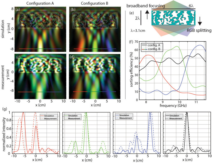
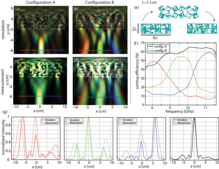
Metasurfaces advanced the field of optics by reducing the thickness of optical components and merging multiple functionalities into a single layer device. However, this generally comes with a reduction in performance, especially for multi-functional and broadband applications. Three-dimensional metastructures can provide the necessary degrees of freedom for advanced applications, while maintaining minimal thickness. This work explores mechanically reconfigurable devices that perform focusing, spectral demultiplexing, and polarization sorting based on mechanical configuration. As proof of concept, a rotatable device, a device based on rotating squares, and a shearing-based device are designed with adjoint-based topology optimization, 3D-printed, and measured at microwave frequencies (7.6-11.6 GHz) in an anechoic chamber.


Conflict of interest statement

The authors declare no competing interests.

Figures

Figure 1
Figure 1
The anechoic chamber used to measure the 3D printed devices. (a) A sideview of the chamber. A TEM mode is injected into the anechoic chamber, exciting the device at approximately normal incidence. The fields in the cavity, including fields above the device, are measured with a small antenna probe extending through the top aluminum plate. The bottom aluminum plate is scanned in two directions to make a full 2D scan. (b) A picture of the anechoic chamber with the top aluminum plate removed. The scanning area is surrounded by absorbing foam. Triangles were cut out of the absorbing foam to reduce reflections. (c) A schematic representation of the measurement setup. The microwave source (Windfreak SynthHD) is scanned from 7.6 to 11.6 GHz and is injected through a waveguide adapter. The signal from the measurement probe is first amplified with two low-noise amplifiers, and the signal is then passed through a Schottky power detector (Keysight 8470B). The output is proportional to the field amplitude in the cavity.
Figure 2
Figure 2
Rotatable device performing broadband focusing in one configuration and spectral splitting in the other configuration. (a) Broadband focusing simulation, (b) spectral splitting simulation, (c) broadband focusing measurement, and (d) spectral splitting measurement. (e) Schematic of the device, where blue represents PLA and white represents air. The footprint of the device is 6.2 cm × 18.6 cm. (f) Analysis of the simulated fields at the focal plane showing the sorting efficiency for each function, defined as the fraction of incident power reaching the target pixel. Red, green, and blue light are focused to their respectively colored pixels, and sorting efficiency is drawn in red, green, and blue, respectively. The broadband focusing function focuses all light to the middle pixel and is drawn in black. (g) Comparison of simulated and measurement normalized intensity profiles at the focal plane. Configuration B intensities are integrated over (left) 7.6–8.9 GHz, (center-left) 8.9–10.2 GHz, (center-right) 10.2–11.6 GHz. (right) Configuration A intensity integrated from 7.6 to 11.6 GHz.
Figure 3
Figure 3
The device performing broadband focusing in one configuration and spectral splitting in the other configuration. (a) Broadband focusing simulation, (b) spectral splitting simulation, (c) broadband focusing measurement, and (d) spectral splitting measurement. (e) Demonstration of the transformation and device footprint, where blue represents PLA and white represents air. The footprint of the device is 6.2 cm × 18.6 cm. (f) Analysis of the focal plane of this device, showing the sorting efficiency for each function, defined as the fraction of incident power reaching the target pixel. Red, green, and blue light are focused to their respectively colored pixels, and sorting efficiency is drawn in red, green, and blue, respectively. The broadband focusing function focuses all light to the middle pixel and is drawn in black. (g) Comparison of simulated and measured normalized intensity profiles at the focal plane. Configuration B intensities are integrated over (left) 7.6–8.9 GHz, (center-left) 8.9–10.2 GHz, (center-right) 10.2–11.6 GHz. (right) Configuration A intensity integrated from 7.6 to 11.6 GHz.
Figure 4
Figure 4
TE and TM fields for a device based on a net shearing movement of 6 cm. (a) The spectral splitting configuration splits red, green, and blue light to the red, green, and blue pixels, respectively. This is analyzed for both TE and TM polarizations. (b) The neutral state of the device performs broadband focusing to the center pixel for both TE and TM polarizations. (c) The polarization sorting configuration sorts broadband TE light to the left (red) pixel and focuses broadband TM light to the center (green) pixel. (df) Sorting efficiency of the different configurations. The line color represents the sorting efficiency to the similarly colored pixel as depicted in the color plots. Solid lines represent the TE response, and dashed lines represent the TM response. (d) Sorting efficiency in the spectral splitting configuration. (e) Sorting efficiency for the broadband focusing configuration. (f) Sorting efficiency for the polarization splitting configuration. (Inset) A confusion matrix representation of the sorting efficiency, with true input on the vertical axis and predicted input on the horizontal axis. Each matrix entry is determined by averaging the relevant trace over the full bandwidth.

References

    1. Yu N, Capasso F. Flat optics with designer metasurfaces. Nat. Mater. 2014;13:139–150. doi: 10.1038/nmat3839. - DOI - PubMed
    1. Kamali SM, Arbabi E, Arbabi A, Faraon A. A review of dielectric optical metasurfaces for wavefront control. Nanophotonics. 2018;7:1041–1068. doi: 10.1515/nanoph-2017-0129. - DOI
    1. Miller DAB. Fundamental limit for optical components. J. Opt. Soc. Am. B. 2007;24:A1. doi: 10.1364/JOSAB.24.0000A1. - DOI
    1. Arbabi A, Faraon A. Fundamental limits of ultrathin metasurfaces. Sci. Rep. 2017;7:1–9. doi: 10.1038/srep43722. - DOI - PMC - PubMed
    1. Arbabi A, Arbabi E, Horie Y, Kamali SM, Faraon A. Planar metasurface retroreflector. Nat. Photonics. 2017;11:415–420. doi: 10.1038/nphoton.2017.96. - DOI