

Charge Transport in and Electroluminescence from sp3-Functionalized Carbon Nanotube Networks
- PMID: 34048654
- PMCID: PMC8223481
- DOI: 10.1021/acsnano.1c02878
Charge Transport in and Electroluminescence from sp3-Functionalized Carbon Nanotube Networks
Abstract
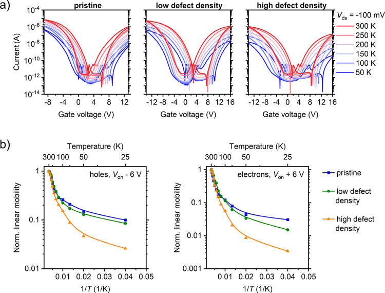
The controlled covalent functionalization of semiconducting single-walled carbon nanotubes (SWCNTs) with luminescent sp3 defects leads to additional narrow and tunable photoluminescence features in the near-infrared and even enables single-photon emission at room temperature, thus strongly expanding their application potential. However, the successful integration of sp3-functionalized SWCNTs in optoelectronic devices with efficient defect state electroluminescence not only requires control over their emission properties but also a detailed understanding of the impact of functionalization on their electrical performance, especially in dense networks. Here, we demonstrate ambipolar, light-emitting field-effect transistors based on networks of pristine and functionalized polymer-sorted (6,5) SWCNTs. We investigate the influence of sp3 defects on charge transport by employing electroluminescence and (charge-modulated) photoluminescence spectroscopy combined with temperature-dependent current-voltage measurements. We find that sp3-functionalized SWCNTs actively participate in charge transport within the network as mobile carriers efficiently sample the sp3 defects, which act as shallow trap states. While both hole and electron mobilities decrease with increasing degree of functionalization, the transistors remain fully operational, showing electroluminescence from the defect states that can be tuned by the defect density.
Keywords: charge modulation spectroscopy; covalent functionalization; electroluminescence; light-emitting field-effect transistors; single-walled carbon nanotubes; sp3 defects.
Conflict of interest statement
The authors declare no competing financial interest.
Figures


Similar articles
-
Tuning Electroluminescence from Functionalized SWCNT Networks Further into the Near-Infrared.ACS Appl Opt Mater. 2023 Oct 16;1(10):1706-1714. doi: 10.1021/acsaom.3c00261. eCollection 2023 Oct 27. ACS Appl Opt Mater. 2023. PMID: 37915970 Free PMC article.
-
Probing Carrier Dynamics in sp3-Functionalized Single-Walled Carbon Nanotubes with Time-Resolved Terahertz Spectroscopy.ACS Nano. 2022 Jun 28;16(6):9401-9409. doi: 10.1021/acsnano.2c02199. Epub 2022 Jun 16. ACS Nano. 2022. PMID: 35709437 Free PMC article.
-
Guiding Charge Transport in Semiconducting Carbon Nanotube Networks by Local Optical Switching.ACS Appl Mater Interfaces. 2020 Jun 24;12(25):28392-28403. doi: 10.1021/acsami.0c05640. Epub 2020 Jun 11. ACS Appl Mater Interfaces. 2020. PMID: 32476400
-
Advances in NO2 sensing with individual single-walled carbon nanotube transistors.Beilstein J Nanotechnol. 2014 Nov 20;5:2179-91. doi: 10.3762/bjnano.5.227. eCollection 2014. Beilstein J Nanotechnol. 2014. PMID: 25551046 Free PMC article. Review.
-
Recent progress in controlling the photoluminescence properties of single-walled carbon nanotubes by oxidation and alkylation.Chem Commun (Camb). 2023 Dec 7;59(98):14497-14508. doi: 10.1039/d3cc05065c. Chem Commun (Camb). 2023. PMID: 38009193 Review.
Cited by
-
Unraveling aryl peroxide chemistry to enrich optical properties of single-walled carbon nanotubes.Chem Sci. 2024 Dec 11;16(3):1374-1389. doi: 10.1039/d4sc04785k. eCollection 2025 Jan 15. Chem Sci. 2024. PMID: 39703412 Free PMC article.
-
Carbon Nanotube Devices for Quantum Technology.Materials (Basel). 2022 Feb 18;15(4):1535. doi: 10.3390/ma15041535. Materials (Basel). 2022. PMID: 35208080 Free PMC article. Review.
-
Unified Quantification of Quantum Defects in Small-Diameter Single-Walled Carbon Nanotubes by Raman Spectroscopy.ACS Nano. 2023 Nov 14;17(21):21771-21781. doi: 10.1021/acsnano.3c07668. Epub 2023 Oct 19. ACS Nano. 2023. PMID: 37856164 Free PMC article.
-
How to recognize clustering of luminescent defects in single-wall carbon nanotubes.Nanoscale Horiz. 2024 Nov 19;9(12):2286-2294. doi: 10.1039/d4nh00383g. Nanoscale Horiz. 2024. PMID: 39380328 Free PMC article.
-
Absolute Quantification of sp3 Defects in Semiconducting Single-Wall Carbon Nanotubes by Raman Spectroscopy.J Phys Chem Lett. 2022 Apr 28;13(16):3542-3548. doi: 10.1021/acs.jpclett.2c00758. Epub 2022 Apr 14. J Phys Chem Lett. 2022. PMID: 35420437 Free PMC article.
References
-
- Avouris P.; Freitag M.; Perebeinos V. Carbon-Nanotube Photonics and Optoelectronics. Nat. Photonics 2008, 2, 341–350. 10.1038/nphoton.2008.94. - DOI
-
- Liang S.; Wei N.; Ma Z.; Wang F.; Liu H.; Wang S.; Peng L.-M. Microcavity-Controlled Chirality-Sorted Carbon Nanotube Film Infrared Light Emitters. ACS Photonics 2017, 4, 435–442. 10.1021/acsphotonics.6b00856. - DOI
LinkOut - more resources
Full Text Sources
Other Literature Sources
