. 2021 May 20;12(5):583.
doi: 10.3390/mi12050583.

Morphological Study of Nanostructures Induced by Direct Femtosecond Laser Ablation on Diamond

Affiliations

Morphological Study of Nanostructures Induced by Direct Femtosecond Laser Ablation on Diamond

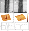
Ahmed Abdelmalek et al. Micromachines (Basel). .

Abstract

High spatial frequency laser induced periodic surface structure (HSFL) morphology induced by femtosecond laser with 230 fs pulse duration, 250 kHz repetition rate at 1030 nm wavelength on CVD diamond surface is investigated and discussed. The spatial modification was characterized and analyzed by Scanning Electron Microscopy (SEM), Atomic Force Microscopy (AFM) and 2D-Fast Fourier Transform (2D-FFT). We studied the effect of pulse number and laser power on the spatial development of nanostructures, and also deduced the impact of thermal accumulation effect on their morphology. A generalized plasmonic model has been used to follow the optical evolution of the irradiated surface and to determine the periodic value of the nanostructures. We suggest that non-thermal melting and plasmonic excitation are the main processes responsible for the formation of HSFL-type nanostructures.

Keywords: 2D-FFT; LIPSS morphology; femtosecond laser; plasmonic excitation.


Conflict of interest statement

The authors declare no conflict of interest.

Figures

Figure 1
Figure 1
Schematic layout of the femtosecond laser writing setup.
Figure 2
Figure 2
Summary of the modification results obtained during diamond surface irradiation by multipulse femtosecond laser for varying laser fluence and number of pulses.
Figure 3
Figure 3
Representation of effect of pulse number on the morphology of the diamond surface irradiated by fs laser pulses with power of P = 19 mW (F=7.56J/cm2). (ac) shows planar view SEM images of structures induced by N = 89, 100 and 133 pulses. (df) AFM measurements recorded in tapping mode of the (ac), respectively (measured area 5 × 5 μm2). (gi) represent the cross-section profile corresponding to the lines marked in (df), respectively. (jl) represent 2D-fast Fourier transforms (2D-FFT) and (mo) its cross section horizontal profiles, respectively. The double-arrow shows the polarization of the incident laser beam.
Figure 3
Figure 3
Representation of effect of pulse number on the morphology of the diamond surface irradiated by fs laser pulses with power of P = 19 mW (F=7.56J/cm2). (ac) shows planar view SEM images of structures induced by N = 89, 100 and 133 pulses. (df) AFM measurements recorded in tapping mode of the (ac), respectively (measured area 5 × 5 μm2). (gi) represent the cross-section profile corresponding to the lines marked in (df), respectively. (jl) represent 2D-fast Fourier transforms (2D-FFT) and (mo) its cross section horizontal profiles, respectively. The double-arrow shows the polarization of the incident laser beam.
Figure 4
Figure 4
3D view of top LIPSS shown in Figure 3d showing the roughness of the nanowalls. (a) shows a side view taken after the etching as represented in top view in (b).
Figure 5
Figure 5
Representation of effect of laser fluence on the morphology of the diamond surface irradiated by 89 pulses (4.5 mm/s). (a,b) shows SEM images induced by 7.16 and F=7.96J/cm2, respectively. (c,d) AFM measurements of the (a,b), respectively (measured area 5 × 5 μm2). (e,f) represent the cross-section profile corresponding to the lines marked in (c,d), respectively. The double-arrow shows the polarization of the incident laser beam.
Figure 6
Figure 6
Evolution of periodicity of HSFL nanostructure with pulse number and laser power at 1030 nm wavelength.
Figure 7
Figure 7
Dielectric function of diamond in function to electron plasma excitation by fs-laser at 1030 nm wavelength. RPmin and RPmax represent the resonance plasmonic in pseudo-metal/air and pseudo-metal/diamond interface, respectively.
Figure 8
Figure 8
(top) reflectivity and (bottom) laser penetration depth of diamond in function of electron plasma excitation. The penetration depth corresponding to plasmonic excitation range is shown in the inset.
Figure 9
Figure 9
Calculation of LIPSS period evolution as a function of electron plasma excitation at pseudo-metal/air interface (m=0) and pseudo-metal/diamond interface (m=1) under fs-laser irradiation at 1030 nm wavelength. Optical system modeled as a pseudo-metal layer surrounded by the original material (diamond) and air is shown in the inset.
Figure 10
Figure 10
A proposed scenario for HSFL formation during multipulse femtosecond laser irradiation.

References

    1. Gattass R.R., Mazur E. Femtosecond laser micromachining in transparent materials. Nat. Photonics. 2008;2:219–225. doi: 10.1038/nphoton.2008.47. - DOI
    1. Mottay E., Liu X., Zhang H., Mazur E. Industrial applications of ultrafast laser processing. MRS Bull. 2016;41:984–992. doi: 10.1557/mrs.2016.275. - DOI
    1. Chichkov B.N., Momma C., Nolte S., von Alvensleben F., Tünnermann A. Femtosecond, picosecond and nanosecond laser ablation of solids. Appl. Phys. A. 1996;63:109–115. doi: 10.1007/BF01567637. - DOI
    1. Bonse J., Hohm S., Kirner S.V., Rosenfeld A., Kruger J. Laser-Induced Periodic Surface Structures—A Scientific Evergreen. IEEE J. Sel. Top. Quantum Electron. 2016;23:9000615. doi: 10.1109/JSTQE.2016.2614183. - DOI
    1. Wu Q., Ma Y., Fang R., Liao Y., Yu Q., Chen X., Wang K. Femtosecond laser-induced periodic surface structure on diamond film. Appl. Phys. Lett. 2003;82:1703–1705. doi: 10.1063/1.1561581. - DOI

LinkOut - more resources