Review
. 2021 May 29;12(6):634.
doi: 10.3390/mi12060634.

Additive Manufacture of Small-Scale Metamaterial Structures for Acoustic and Ultrasonic Applications

Affiliations
Review

Additive Manufacture of Small-Scale Metamaterial Structures for Acoustic and Ultrasonic Applications

Alicia Gardiner et al. Micromachines (Basel). .

Abstract

Acoustic metamaterials are large-scale materials with small-scale structures. These structures allow for unusual interaction with propagating sound and endow the large-scale material with exceptional acoustic properties not found in normal materials. However, their multi-scale nature means that the manufacture of these materials is not trivial, often requiring micron-scale resolution over centimetre length scales. In this review, we bring together a variety of acoustic metamaterial designs and separately discuss ways to create them using the latest trends in additive manufacturing. We highlight the advantages and disadvantages of different techniques that act as barriers towards the development of realisable acoustic metamaterials for practical audio and ultrasonic applications and speculate on potential future developments.

Keywords: acoustic metamaterials; acoustics; additive manufacturing; ultrasonics.


Conflict of interest statement

The authors declare no conflict of interest.

Figures

Figure 1
Figure 1
Pendry’s artificial microstructure design for manipulating low-frequency plasmons. Reprinted with permission from [43] (As follows: [J. B. Pendry et al., Physical Review Letters, Volume 76, Pages 4773–4776, 1996.], copyright (1996) by the American Physical Society).
Figure 2
Figure 2
Omni-directional 3D acoustic cloak manufactured using 3D printing (cloak operational for acoustic waves at a frequency of 3 kHz) [57]. (Reprinted by permission from Springer Nature: [Nature Materials, ‘Three-dimensional broadband omnidirectional acoustic ground cloak’, L. Zigoneanu et al., 2014]).
Figure 3
Figure 3
An FEA plot of sound pressure level of a Matryoshka locally resonant sonic crystal, modelled using COMSOL Multiphysics. Sound pressure levels are relatively consistent throughout when the incident wave has a frequency of 2 kHz (top) and lies outside the band gap but are attenuated considerably at 4 kHz (bottom) inside the gap.
Figure 4
Figure 4
Examples of inertial meta-atom structures: with (a) showing a matrix of coated spherical inclusions (From [67]. Reprinted with permission from AAAS). Displayed in (b) are various configurations of Helmholtz resonator arrays [68] (Reprinted from Applied Acoustics, Volume 155, D.P. Jena, J. Dandsena, V.G. Jayakumari, ‘Demonstration of effective acoustic properties of different configurations of Helmholtz’, Pages 371-382, Copyright (2019), with permission from Elsevier).
Figure 5
Figure 5
Examples of AMM devices incorporating membranes and perforated plates, where (a) displays a uniform metastructure of hexagonal unit-cells arranged in parallel and sealed by membranes at each open end (Reprinted from [71], with the permission of AIP Publishing). (b) shows a perforated thin-plate design with holes drilled at the cross points of the resin frame to introduce anti-resonant behaviour [73] (Republished with permission of IOP Publishing Ltd., from [Journal of Physics D: Applied Physics, Y. Xu, et al., Volume 52, Edition No. 40, 2019.]; permission conveyed through Copyright Clearance Center, Inc., Danvers, MA, USA).
Figure 6
Figure 6
A 2D coiled structure acoustic metasurface [82].
Figure 7
Figure 7
Coiled acoustic metamaterial structures in (a) 2D and (b) 3D, showing the equivalent cells in each case [85].
Figure 8
Figure 8
Broadband enhancement examples using acoustic metasurfaces. (A) displays a gradient coiled metamaterial with (ac) presenting the design at various angles and cross-sections and (d) showing a diagram of the acoustic boundaries [86] (Republished with permission of IOP Publishing Ltd., from [Journal of Physics D: Applied Physics, T. Chen, et al., Volume 54, 2020.]; permission conveyed through Copyright Clearance Center, Inc.). (B) shows a 3D-printed fractal metamaterial design (Reprinted from [87], with the permission of AIP Publishing).
Figure 9
Figure 9
(a) Initial experimental prototype of an active AMM cell comprised of an acrylic cylinder with piezoelectric bimorphs sealing the ends. The volume of the cell is filled with water to act as the transmission medium. The piezoelectric membranes act as both actuators and sensing apparatus; hence they are connected via electrodes to a controller and amplifier (Reprinted from [38], with the permission of AIP Publishing). (b) Experimental set-up for an active AMM cell using piezoelectric membranes. A similar but more refined version of the experimental prototype in (a), with this example being more compact with additional embedded pressure sensors and closed-loop control [88] (Reprinted from Applied Acoustics, Volume 178, W. Akl and A. Baz., ‘Active control of the dynamic density of acoustic metamaterials’, Copyright (2021), with permission from Elsevier).
Figure 10
Figure 10
Tuneable Helmholtz resonator showing (a) a rendering of an experimental metamaterial design, composed of tuneable Helmholtz resonators that are actuated by inflatable balloons, (b) the variations of the plunger clearance depicted with the balloon inflated and deflated and (c) clearances as shown in the experimental prototype [92].
Figure 11
Figure 11
Structure of the active meta-unit with an electromagnetic tuning mechanism. A membrane is tensioned using electromagnetically-operated clamps attached to the pipe exterior [33].
Figure 12
Figure 12
Metagel design consisting of microstructure channels in a tough hydrogel matrix. The acoustic impedance of the hydrogel matches well with water, resulting in almost total transmission of incident waves. These channels can be filled with various liquids to modulate the presenting transmission characteristics of the metagel. In the figure, (A) shows “no channels”, with almost total acoustic transmission; (B) shows “water-filled channels”, with almost total acoustic transmission; (C) shows “air-filled channels”, with almost total acoustic reflection; and (D) shows “liquid gallium-filled channels”, with combined transmission and reflection characteristics. (Reprinted from [93], with the permission of John Wiley & Sons Inc.).
Figure 13
Figure 13
Lattice comprised of hydrogel-composite meta-units, with successive stages of hydration displayed. Here, the scale bar length equates to 5 mm. The initial state is shown at ambient conditions, before immersion in water for 45 min, followed by dehydration via a drying oven set at 75 °C for 35 min [36].
Figure 14
Figure 14
Electron microscope image of a seahorse feature printed using an optimized SLA technique. The right-side image has the predicted shape superimposed. The scale bar here equates to 1 μm [107]. (Reprinted from IFAC-PapersOnLine, Volume 50, Issue 1, A. Fleming, et al., ‘Experimental Scanning Laser Lithography with Exposure Optimization’, Pages 8662-8667, Copyright (2017), with permission from IFAC).
Figure 15
Figure 15
Assembly process of a hydrogel micro-SLA-printed bio-bot, actuated with skeletal muscle. The biobot (i) is placed within the holder (ii), and the assembly (iii) is filled with the cell-matrix solution. This material is compacted around the biobot pillars to form a solid muscle strip (v) and with immunostaining (vi). The final device is shown in the bottom-right. All scale bars here are 1 mm [104].
Figure 16
Figure 16
Micro-SLA-fabricated 3D cross-shape, printed with multicolour resins. The modelled CAD geometry is shown from orthogonal (a) and top-view (b) angles alongside the finished part at orthogonal (c) and top view (d) angles. Here, scale bars are 200 μm [111].
Figure 17
Figure 17
A micro-beam fabricated with DLP using clear IP-S resin photopolymer, where the smallest non-support feature is 86.7 μm. Twenty supports with a diameter of 3 μm were used during the building process. Here, the scale bar is 200 μm [114].
Figure 18
Figure 18
Gyroid structure printed in microscale with DLP showing (A) a diagram of the DLP set-up; (B) the gyroid part, printed at 500 mm/h; and (C) ramp test prints with slice thicknesses of 100 μm, 25 μm and 1 μm, successively. (From [115], Reprinted with permission from AAAS).
Figure 19
Figure 19
Test print for a multi-material DLP method using red and yellow photocurable resin (Reprinted from [116], with author permission).
Figure 20
Figure 20
Multi-material printed part using DLP with UV and visible light exposure, where (a) shows the geometry of the part with UV irradiated sections highlighted in purple, and (b) shows the finished print with (left) no thermal post-cure and (right) 3-h thermal post-cure at 60 °C. Here, the scale bar represents 12 mm [120].
Figure 21
Figure 21
“Notre Dame” printed part using the novel tomographic multi-beam method. The scale bars are 5 mm in the main image, and 1 mm for the inset [122].
Figure 22
Figure 22
MPP-printed 150 μm3 cube of replica shale rock with nanoscale features, where the image is taken with an electron microscope [15].
Figure 23
Figure 23
Nanoscale woodpile structures printed with MPP showing (a) laser excitation of 0.6 μW and a resultant beam thickness of 72 nm, and (b) laser excitation of 0.45 μW and a resultant beam thickness of 60 nm [126].
Figure 24
Figure 24
Microscope image of red blood cells filtered from plasma with a micro-porous filter, printed with MPP [138]. (Republished with permission of Royal Society of Chemistry, from [Lab on a chip, L. Amato, et al., Volume 12, Issue 6, Pages 1135-1142, 2012]; permission conveyed through Copyright Clearance Center, Inc).
Figure 25
Figure 25
Geometry of a micro-perforated plate fabricated with SLS [140].
Figure 26
Figure 26
A lightweight panel-based AMM structure, with each panel comprised of 8 by 8 locally-resonant unit-cells and fabricated using SLS, showing (a) the schematic of a single panel, with an inset section displaying the geometry of a single unit-cell, (b) a diagram of the prototype, where the panels are arranged in a box shape and then housed by a solid material border, and (c) the experimental setup to measure the acoustic response of the printed prototype [141]. (Reprinted from Mechanical Systems and Signal Processing, Volume 70, C. Claeys, et al., ‘A lightweight vibro-acoustic metamaterial demonstrator: Numerical and experimental investigation’, Pages 853-880, Copyright (2016), with permission from Elsevier).
Figure 27
Figure 27
Three distinct printed designs of a 3D soft, auxetic lattice structure, commonly referred to as a Bucklicrystal. These crystal lattices all were SLS-printed using TPU powder and with 60% porosity and show (a) a crystal lattice with body-centred-cubic unit-cells with 6 holes, (b) a crystal lattice with cubic solid-centred unit-cells with 12 holes, and (c) a crystal lattice with body-centred-cubic unit-cells with 12 holes. Here, the scale bar equates to 1 cm [142]. (Reprinted from Materials & Design, Volume 120, S. Yuan, et al., ‘3D soft auxetic lattice structures fabricated by selective laser sintering: TPU powder evaluation and process optimization’, Pages 317-327, Copyright (2017), with permission from Elsevier).
Figure 28
Figure 28
An SLM-fabricated micro-needle for drug delivery applications, where the needle was constructed from 316L stainless steel powder, with a length of 550 μm and an interior aperture measuring 160 μm across [145].
Figure 29
Figure 29
Cross-section of optimized lattice design printed using SLM with Ti-6Al-4V powder. The bottom middle panel displays the pattern geometry with two alternating periodic spacings. The remaining panels (ae) respectively show labelled and magnified images of the lattice in the microscale, where the scale bar is 500 μm [148]. (Reprinted from Journal of Manufacturing Processes, Volume 56, L. Zhang, et al., ‘Topology-optimized lattice structures with simultaneously high stiffness and light weight fabricated by selective laser melting: Design, manufacturing and characterization’, Pages 1166–1177, Copyright (2020), with permission from Elsevier).
Figure 30
Figure 30
The design of an acoustic metamaterial panel that uses local resonance to attenuate sound, where the panel consists of a 2D array of unit-cells held in place by a solid border. These unit-cells consist of a clover-shaped mass inclusion connected to thin structural supports. The figure shows (a) the schematics of the panel design, with dimensions shown in mm, (b) the displacement plot of a single meta-cell during attenuation peak at 1050 Hz, and (c) the displacement plot of a single meta-cell during transmission peak at 1380 Hz [151]. (Used with permission of American Society of Mechanical Engineers, from [151] [‘Experimental and Numerical Assessment of Local Resonance Phenomena in 3D-Printed Acoustic Metamaterials’, Journal of vibration and acoustics, D. Roca, et al., Volume 142, Issue 2, 2020.]; permission conveyed through Copyright Clearance Center, Inc.).
Figure 31
Figure 31
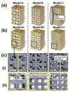
Digital images of three different micro-lattice designs (a) with and (b) without solid outer supports on the edges. The unit-cells of Models A to C are progressively smaller in size, with cell lengths ranging from 3.33 mm to 2 mm. The supports for models A+ to C+ also range in thicknesses from 670 μm to 400 μm. Sub-figure (c) shows magnified sections of the models displayed in (a,b), with focus on the smaller (c)—(i) and larger (c)—(ii) pore structures. Here, the scale bar is 3 mm [152]. (Reprinted from Additive Manufacturing, Volume 36, P. Wang, et al., ‘Electron beam melted heterogeneously porous microlattices for metallic bone applications: Design and investigations of boundary and edge effects’, Copyright (2020), with permission from Elsevier).
Figure 32
Figure 32
A uniform, chiral structure made of copper shown (a) without and (b) with a rubber encasing. The hybrid composite structure (b) combines the initial EBM-bonded copper lattice with a silicon polymer filler while maintaining a vacuum seal of 0.5 MPa in the build chamber during fabrication [153]. (Reprinted from Composite Structures, Volume 234, N. Novak, et al., ‘Mechanical properties of hybrid metamaterial with auxetic chiral cellular structure and silicon filler’, Copyright (2020), with permission from Elsevier).
Figure 33
Figure 33
Microscopic images of zirconia lattices printed via freeform extrusion, with (a) 300 μm and (b) 70 μm size pores. Here, the scale bar is 200 μm [158].
Figure 34
Figure 34
A fine ceramic (calcium phosphate) lattice printed via freeform extrusion and with a mesh spacing/pore size of 70 μm. Calcium phosphate is biocompatible and commonly used as bone substitution material. Here, the scale bar size is 500 μm. (Reprinted from [154], with the permission of John Wiley & Sons Inc).
Figure 35
Figure 35
Carbon nanotube prototype with woven structure printed via liquid deposition modelling (a variant of FDM). The microstructure is displayed from (a) a top view and (b) a side view, with scale bars of 100 μm and 30 μm, respectively, and (c) shows the experimental confirmation of the prototypes electrical properties by connecting it to a simple electric circuit that lights up an LED [159]. (Reprinted from Composites Part A: Applied Science and Manufacturing, Volume 76, G. Postiglione, et al., ‘Conductive 3D microstructures by direct 3D printing of polymer/carbon nanotube nanocomposites via liquid deposition modeling’, Pages 110–114, Copyright (2015), with permission from Elsevier).
Figure 36
Figure 36
A metallic circular microstructure made using DIW with highly concentrated silver nanoparticle ink. The structure was fabricated layer-by-layer with continuous ink deposition and has a minimum feature size of 2 μm. Here, the scale bar is 200 μm. (Reprinted from [155], with the permission of John Wiley & Sons Inc.).
Figure 37
Figure 37
Magnification of hollow “woodpile” microstructure. The lattice design is made of silicon and formed using a direct ink written polymer scaffold that was then silicon-coated and melted to produce the hollow structure. The lattice is 8 by 8 with lateral dimensions of 250 μm by 250 μm. (A) Magnified image of lattice architecture with a scale bar of 5 μm. (B) Magnified image with a scale bar of 500 nm]. (Reprinted from [161], with the permission of John Wiley & Sons Inc.).
Figure 38
Figure 38
An DIW-fabricated vascularised tissue, with thickness exceeding 1 cm, printed in a 3D perfusion chip, showing (a) the chip that is printed in silicon and that enables perfusion within the tissue to occur for long time periods (greater than 6 weeks), and (b) the tissue, which is a multicellular matrix with embedded vascular structures (coloured red in the image). This tissue was constructed by co-printing several inks, which were composed of live cells (such as human stem cells and dermal fibroblasts) [162].
Figure 39
Figure 39
An AMM unit-cell for superior sound attenuation, fabricated using polyjet technology with polymer ink. The unit-cell is contained within a 50 mm wide cubic volume, with the printed prototype being 200 mm by 200 mm by 50 mm and containing 16 unit-cells [163]. (Reprinted from Procedia Engineering, Volume 176, R. Vdovin, et al., ‘Implementation of the Additive PolyJet Technology to the Development and Fabricating the Samples of the Acoustic Metamaterials’, Pages 595–599, Copyright (2017), with permission from Elsevier).
Figure 40
Figure 40
A cylindrical microstructure printed using EHD jetting with a novel electrostatic deflection system. The part was fabricated from polyethylene oxide (PEO) ink and achieved a submicron feature size without the use of supports. Here, a scale bar of (a) 5 μm and (b) 1 μm are used to image the microstructure [164].
Figure 41
Figure 41
Several soft robot prototypes printed with a DLP–DIW hybrid method, with the four structure designs shown in (be) and a colour-coded key for the different materials in (a). These active structures are shown after printing (left), during heating/actuation (middle), and after cooling/relaxation (right). The structures are printed with layer thicknesses of 50 μm (for the DLP polymer matrix) and 700 μm (for the DIW LCE fibres), and the scale bar is 10 mm [165]. (Reprinted from Additive Manufacturing, Volume 40, X. Peng, et al., ‘Integrating digital light processing with direct ink writing for hybrid 3D printing of functional structures and devices’, Copyright (2021), with permission from Elsevier).
Figure 42
Figure 42
An example of a hydrophilic “egg-beater” microstructure printed using a DLP-based printing method, showing (a) the CAD model, and (b) an electron microscope image of the printed part, where the scale bar is 100 μm (top) and 200 μm (bottom). (Reprinted from [166], with the permission of John Wiley & Sons Inc.).
Figure 43
Figure 43
Cross-section of molten PA12 after 10 s simultaneous melting by a thulium laser, which is an integral step in the SLBM fabrication process. This study uses polypropylene (PP) and polyamide 12 (PA12) powder to print a multi-material part, where the resulting layer thickness is 175 μm. (Reprinted with permission from [167]. Copyright (2015), Laser Institute of America).
Figure 44
Figure 44
The geometry of the flattened Luneburg lens designs, fabricated using polyjet technology, showing (a) the periodic unit-cell of both lenses with dimensional variables appropriately labelled—this proposed building block can form a uniform 3D lattice once connected to adjacent, identical unit-cells; and (b) the 2D and (c) 3D lens designs printed with 5 and 19 stacked layers, respectively. (Reprinted from [168], with the permission of AIP Publishing).

Similar articles

Cited by

References

    1. Olsson Iii R.H., El-Kady I. Microfabricated phononic crystal devices and applications. Meas. Sci. Technol. 2008;20:012002. doi: 10.1088/0957-0233/20/1/012002. - DOI
    1. Fritzler K.B., Prinz V.Y. 3D printing methods for micro- and nanostructures. Phys. Uspekhi. 2019;62:54–69. doi: 10.3367/UFNe.2017.11.038239. - DOI
    1. Lee D., Nguyen D.M., Rho J. Acoustic wave science realized by metamaterials. Nano Converg. 2017;4:3. doi: 10.1186/s40580-017-0097-y. - DOI - PMC - PubMed
    1. Panda D., Mohanty A.R. Sonic crystals for highway noise reduction. In: Singh M., Rafat Y., editors. Recent Developments in Acoustics. Springer; Singapore: 2021. pp. 119–128.
    1. Acoustic Metamaterials Group Acousticmetamaterials.org. [(accessed on 13 April 2021)]; Available online: https://acousticmetamaterials.org/

LinkOut - more resources