

A single atom change turns insulating saturated wires into molecular conductors
- PMID: 34103489
- PMCID: PMC8187423
- DOI: 10.1038/s41467-021-23528-8
A single atom change turns insulating saturated wires into molecular conductors
Abstract
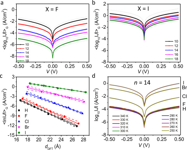
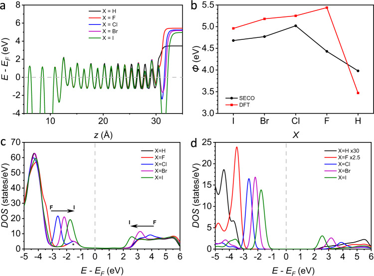
We present an efficient strategy to modulate tunnelling in molecular junctions by changing the tunnelling decay coefficient, β, by terminal-atom substitution which avoids altering the molecular backbone. By varying X = H, F, Cl, Br, I in junctions with S(CH2)(10-18)X, current densities (J) increase >4 orders of magnitude, creating molecular conductors via reduction of β from 0.75 to 0.25 Å-1. Impedance measurements show tripled dielectric constants (εr) with X = I, reduced HOMO-LUMO gaps and tunnelling-barrier heights, and 5-times reduced contact resistance. These effects alone cannot explain the large change in β. Density-functional theory shows highly localized, X-dependent potential drops at the S(CH2)nX//electrode interface that modifies the tunnelling barrier shape. Commonly-used tunnelling models neglect localized potential drops and changes in εr. Here, we demonstrate experimentally that [Formula: see text], suggesting highly-polarizable terminal-atoms act as charge traps and highlighting the need for new charge transport models that account for dielectric effects in molecular tunnelling junctions.
Conflict of interest statement
The authors declare no competing interests.
Figures


Similar articles
-
Interplay of Collective Electrostatic Effects and Level Alignment Dictates the Tunneling Rates across Halogenated Aromatic Monolayer Junctions.J Phys Chem Lett. 2019 Jul 18;10(14):4142-4147. doi: 10.1021/acs.jpclett.9b00387. Epub 2019 Jul 10. J Phys Chem Lett. 2019. PMID: 31260324
-
Tuning the Tunneling Rate and Dielectric Response of SAM-Based Junctions via a Single Polarizable Atom.Adv Mater. 2015 Nov;27(42):6689-95. doi: 10.1002/adma.201502968. Epub 2015 Sep 28. Adv Mater. 2015. PMID: 26414779
-
Coherent tunnelling conductance in magnetic tunnel junctions of half-metallic full Heusler alloys with MgO barriers.J Phys Condens Matter. 2007 Sep 12;19(36):365228. doi: 10.1088/0953-8984/19/36/365228. Epub 2007 Aug 24. J Phys Condens Matter. 2007. PMID: 21694173
-
Influence of halogen substitutions on rates of charge tunneling across SAM-based large-area junctions.Phys Chem Chem Phys. 2015 Jun 7;17(21):13804-7. doi: 10.1039/c5cp00145e. Epub 2015 May 11. Phys Chem Chem Phys. 2015. PMID: 25960312
-
Electron tunneling through alkanedithiol self-assembled monolayers in large-area molecular junctions.Proc Natl Acad Sci U S A. 2007 Jul 3;104(27):11161-6. doi: 10.1073/pnas.0701472104. Epub 2007 Jun 25. Proc Natl Acad Sci U S A. 2007. PMID: 17592120 Free PMC article. Review.
Cited by
-
Gradual Change between Coherent and Incoherent Tunneling Regimes Induced by Polarizable Halide Substituents in Molecular Tunnel Junctions.J Am Chem Soc. 2024 Aug 21;146(33):23356-23364. doi: 10.1021/jacs.4c06295. Epub 2024 Aug 8. J Am Chem Soc. 2024. PMID: 39115108 Free PMC article.
-
Design of Promising Uranyl(VI) Complexes Thin Films with Potential Applications in Molecular Electronics.ChemistryOpen. 2024 Jun;13(6):e202300219. doi: 10.1002/open.202300219. Epub 2024 Jan 5. ChemistryOpen. 2024. PMID: 38180301 Free PMC article.
-
Tuning Overbias Plasmon Energy and Intensity in Molecular Plasmonic Tunneling Junctions by Atomic Polarizability.J Am Chem Soc. 2024 Aug 7;146(31):21642-21650. doi: 10.1021/jacs.4c05544. Epub 2024 Jun 28. J Am Chem Soc. 2024. PMID: 38940772 Free PMC article.
-
An artificial synapse based on molecular junctions.Nat Commun. 2023 Jan 16;14(1):247. doi: 10.1038/s41467-023-35817-5. Nat Commun. 2023. PMID: 36646674 Free PMC article.
-
Interplay between Interfacial Energy, Contact Mechanics, and Capillary Forces in EGaIn Droplets.ACS Appl Mater Interfaces. 2022 Jun 22;14(24):28074-28084. doi: 10.1021/acsami.2c04043. Epub 2022 Jun 1. ACS Appl Mater Interfaces. 2022. PMID: 35649179 Free PMC article.
References
-
- Jortner, J., Nitzan, A. & Ratner, M. A. in Introducing Molecular Electronics (eds. Cuniberti, G. et al.) 13–54 (Springer, 2005).
LinkOut - more resources
Full Text Sources
