. 2021 Jun 15;10(1):125.
doi: 10.1038/s41377-021-00564-z.

Structural and compositional analysis of (InGa)(AsSb)/GaAs/GaP Stranski-Krastanov quantum dots

Affiliations

Structural and compositional analysis of (InGa)(AsSb)/GaAs/GaP Stranski-Krastanov quantum dots

Raja S R Gajjela et al. Light Sci Appl. .

Abstract

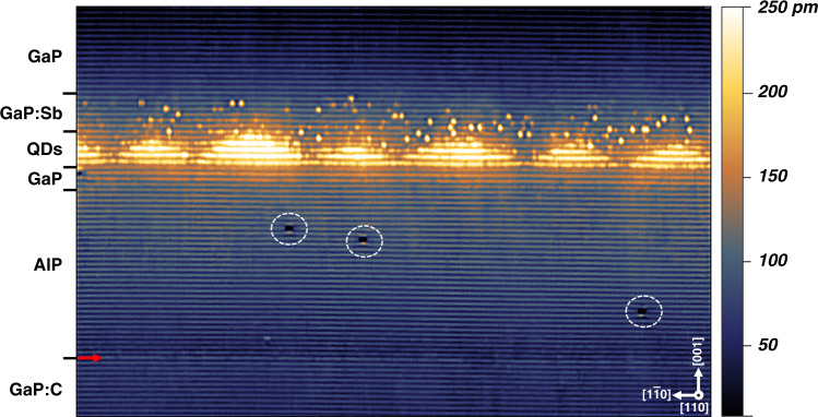
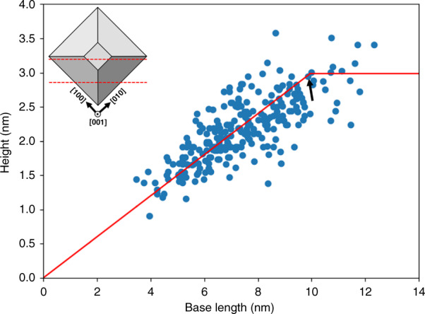
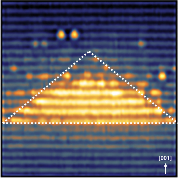
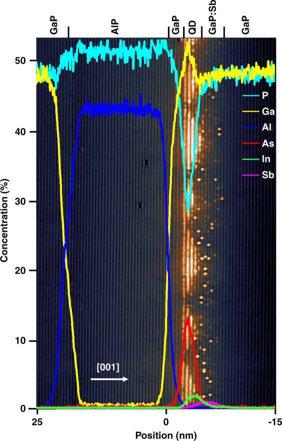
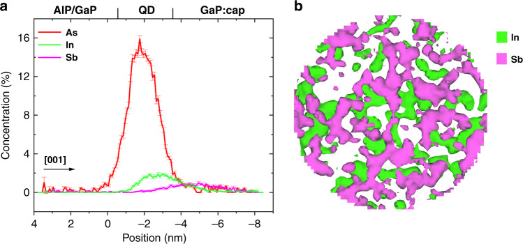
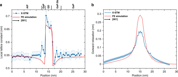
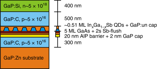
We investigated metal-organic vapor phase epitaxy grown (InGa)(AsSb)/GaAs/GaP Stranski-Krastanov quantum dots (QDs) with potential applications in QD-Flash memories by cross-sectional scanning tunneling microscopy (X-STM) and atom probe tomography (APT). The combination of X-STM and APT is a very powerful approach to study semiconductor heterostructures with atomic resolution, which provides detailed structural and compositional information on the system. The rather small QDs are found to be of truncated pyramid shape with a very small top facet and occur in our sample with a very high density of ∼4 × 1011 cm-2. APT experiments revealed that the QDs are GaAs rich with smaller amounts of In and Sb. Finite element (FE) simulations are performed using structural data from X-STM to calculate the lattice constant and the outward relaxation of the cleaved surface. The composition of the QDs is estimated by combining the results from X-STM and the FE simulations, yielding ∼InxGa1 - xAs1 - ySby, where x = 0.25-0.30 and y = 0.10-0.15. Noticeably, the reported composition is in good agreement with the experimental results obtained by APT, previous optical, electrical, and theoretical analysis carried out on this material system. This confirms that the InGaSb and GaAs layers involved in the QD formation have strongly intermixed. A detailed analysis of the QD capping layer shows the segregation of Sb and In from the QD layer, where both APT and X-STM show that the Sb mainly resides outside the QDs proving that Sb has mainly acted as a surfactant during the dot formation. Our structural and compositional analysis provides a valuable insight into this novel QD system and a path for further growth optimization to improve the storage time of the QD-Flash memory devices.


Conflict of interest statement

The authors declare no competing interests.

Figures

Fig. 1
Fig. 1. A 60 × 40 nm2 filled-state topographic image showing six full QDs taken at a bias voltage: Vb = −3.3 V and a tunnel current: It = 50 pA.
The red arrow indicates the interface between GaP:C and AlP; the white circles indicate “P” vacancies; the dark to bright contrast (250 pm) in the image represents the relative height of the STM tip from the surface as shown to the right of the image in the color bar. The white arrow indicates the growth direction [001]
Fig. 2
Fig. 2. Height vs base length distribution of 261 individual QDs measured from X-STM images.
The red line is a linear fit to the experimental data (blue). The black arrow indicates the position where the shape of the QDs changes from near triangle to trapezium, with a small top facet. On the left corner, the top view of the most probable QD model is given with dotted red lines, indicating the cleaving planes at two different positions
Fig. 3
Fig. 3. A 11 × 11 nm2 filled-state image showing one of the biggest QD taken at Vb = −3.3 V and It = 50 pA with white dotted lines showing a cut through the pyramid.
The diagonal base length of the QD is 11 ± 0.2 nm with a height of 5 BLs and the arrow indicates the growth direction [001]
Fig. 4
Fig. 4. The APT concentration profiles of all the constituent elements (P, Ga, Al, As, In, and Sb) overlaid on top a 40 × 60 nm2 topographic filled-state X-STM image for better visualization and comparison.
The apparent non-stoichiometry of the AlP layer is due to the unresolvable identification issue of complex phosphorus species in the 31 Da peak, as described in “QDs: composition” section. The arrow indicates the growth direction [001] and the different regions are indicated on top of the image
Fig. 5
Fig. 5. APT evaluation of the QD constituent elements.
a APT concentration profile showing only As, In, and Sb is generated from the 30 nm diameter slice shown in panel b rather than from the full dataset that is shown in Fig. 4. The arrow indicates the growth direction [001]; b 30 nm diameter slice of iso-concentration surfaces created with In = 2.0 at.% and Sb = 1.0 at.%, showing the anticorrelation in the spatial distribution of the In- and Sb-rich regions
Fig. 6
Fig. 6. APT investigation of the QD region.
a A 30 nm diameter slice of the iso-concentration surface created with In = 2.0 at.%, showing the In-rich areas, the shaded region represents a 5-nm thick cross-sectional slice taken to plot concentration maps of the elements; b cross-sectional atom map of the shaded region from panel a, showing the distribution of constituent elements (Al, As, In, and Sb); c cross-sectional concentration maps of In and Sb, the dotted lines indicate: (1) In-rich region, (2) In-poor region, and (3) In-poor but As-rich region. The exact composition as reported in the color bars is not completely quantitative due to the spatial blurring from trajectory aberrations that occurs during atom probe, where matrix material from the vicinity of the QDs can appear to be from inside the QDs
Fig. 7
Fig. 7. FE simulations fitting the experimental X-STM results.
a Lattice constant profile of the biggest QD in Fig. 1 (second QD from left) as a function of position in the growth direction (from left to right). The blue points represent the measured lattice constant with an FE simulation in red for a composition of In0.3Ga0.7As0.85Sb0.15. Different layers are marked on top of the profile; b X-STM height profile showing the outward relaxation of the same cleaved QD with an FE simulation in red
Fig. 8
Fig. 8. 40 × 11 nm2 X-STM images of the same area.
a Empty-state image taken at Vb = +3.0 V, It = 90 pA. b Filled-state image taken at Vb = −3.65 V, It = 90 pA. The black arrows indicate the position of Sb atoms in both images, the white triangles indicate some of the subsurface Sb atoms in the filled-state image, the green squares indicate some of the segregated surface In atoms, and the red circle indicates some subsurface In atoms. The dark to bright contrast difference is 250 pm and the arrow on the right side indicates the growth direction [001]
Fig. 9
Fig. 9. Sb concentration as a function of distance in BLs from the wetting layer in the growth direction [001].
The distance from 0 to the dotted line along the x-axis represents the area occupied by the QDs, the dotted line being the top of the QDs. The Sb atoms are counted over a distance of 1 μm on each atomic row, using multiple X-STM filled-state images
Fig. 10
Fig. 10
Schematic structure of the X-STM sample grown by MOVPE

References

    1. Bimberg D, et al. InGaAs-GaAs quantum-dot lasers. IEEE J. Sel. Top. Quant. Electron. 1997;3:196–205. doi: 10.1109/2944.605656. - DOI
    1. Bimberg D. Quantum dots for lasers, amplifiers and computing. J. Phys. D Appl. Phys. 2005;38:2055–2058. doi: 10.1088/0022-3727/38/13/001. - DOI
    1. Müller T, et al. A quantum light-emitting diode for the standard telecom window around 1,550 nm. Nat. Commun. 2018;9:862. doi: 10.1038/s41467-018-03251-7. - DOI - PMC - PubMed
    1. Martín-Sánchez J, et al. single photon emission from site-controlled InAs quantum dots grown on GaAs(001) patterned substrates. ACS Nano. 2009;3:1513–1517. doi: 10.1021/nn9001566. - DOI - PubMed
    1. Yuan ZL. Electrically driven single-photon source. Science. 2002;295:102–105. doi: 10.1126/science.1066790. - DOI - PubMed