Review
. 2021 Jan 4;13(1):49.
doi: 10.1007/s40820-020-00577-0.

Laser Synthesis and Microfabrication of Micro/Nanostructured Materials Toward Energy Conversion and Storage

Affiliations
Review

Laser Synthesis and Microfabrication of Micro/Nanostructured Materials Toward Energy Conversion and Storage

Lili Zhao et al. Nanomicro Lett. .

Abstract

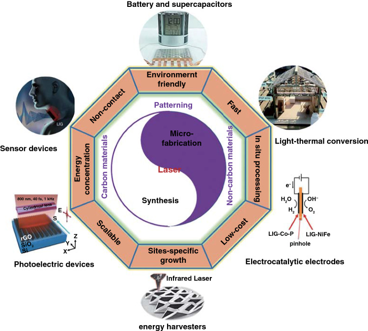
Nanomaterials are known to exhibit a number of interesting physical and chemical properties for various applications, including energy conversion and storage, nanoscale electronics, sensors and actuators, photonics devices and even for biomedical purposes. In the past decade, laser as a synthetic technique and laser as a microfabrication technique facilitated nanomaterial preparation and nanostructure construction, including the laser processing-induced carbon and non-carbon nanomaterials, hierarchical structure construction, patterning, heteroatom doping, sputtering etching, and so on. The laser-induced nanomaterials and nanostructures have extended broad applications in electronic devices, such as light-thermal conversion, batteries, supercapacitors, sensor devices, actuators and electrocatalytic electrodes. Here, the recent developments in the laser synthesis of carbon-based and non-carbon-based nanomaterials are comprehensively summarized. An extensive overview on laser-enabled electronic devices for various applications is depicted. With the rapid progress made in the research on nanomaterial preparation through laser synthesis and laser microfabrication technologies, laser synthesis and microfabrication toward energy conversion and storage will undergo fast development.

Keywords: Energy conversion and storage; Laser microfabrication; Laser synthesis; Micro/nanostructured materials.


Figures

Scheme 1
Scheme 1
Laser as a synthetic technique and a microfabrication technique and their applications in various functional devices
Fig. 1
Fig. 1
a Reduction of GO by laser irradiation utilized a Nd-YAG laser (pulse width in the range of ms) with an excitation wavelength of 1064 nm [21]. b Schematic illustration of ultrathin laser-processed graphene-based micro-planar supercapacitors. After the different powers of laser treatment, the reduction and ablation of GO film were completed [22]. c Representation of positioned laser reduction on one side of a GO fiber. The black region corresponds to the laser-induced G region along the brown GO fiber [23]. d Schematic illustration of the preparation process of graphene bulks and functional counterparts induced by a laser shot within milliseconds [24]. e Schematic of grating processing of a GO film using cylindrical focusing of femtosecond laser pulses. f Photograph (insert) and SEM image of the large-area (10 × 12 mm2) rGO. θ represents the angle between S and E [28]
Fig. 2
Fig. 2
a Manufacturing and processing of laser-induced 3D GFs [37]. b LIG induced from bread, fire-retardant treated pine wood, cotton paper, cardboard box, gray muslin cloth and muslin cloth wrapped around a marker [33]. c Schematic diagram of the laser scribing fabrication of CNS-LSG electrode [42]
Fig. 3
Fig. 3
a Illustration of laser-induced epitaxial graphene synthesis [49]. b Schematic illustration of the synthesis method for laser-induced N-doped graphene on N-doped SiC substrate and cross-sectional HRTEM image of multilayer N-doped graphene on 4H-SiC (0001) [50]. c Schematic diagram of the CO2-laser-induced epitaxial growth of graphene on SiC wafers [51]
Fig. 4
Fig. 4
a Schematic diagram of the optical emission spectroscopy (OES) and laser-induced fluorescence (LIF) setup to characterize the species in the combustion flame with UV laser irradiation. b Schematic illustration of the UV-laser-assisted diamond combustion CVD setup [53]
Fig. 5
Fig. 5
a Digital photograph of Ni plates (10 × 10 cm2) before (left) and after (right) laser ablation and the overall water splitting device by Ni plate. b The applied metals and alloys highlighted within a periodic table [69]. c Various non-noble MNPs produced by the nano-LaMP method in air displayed along with their corresponding MOF crystals. From left to right, the crystal structure of MOFs, optical images, SEM images, PXRD patterns, and XPS patterns of MNPs. HKSUT-1 precursor d and illustrations of the experimental setup e for the nano-LaMP method. f Mechanism for the production of MNPs by laser irradiation on MOFs in air. g Optical image of the MOF crystals prepared for nano-LaMP. The scale bars are inset in g 20 μm and h 200 μm [77]. i Illustration of the laser pyrolysis process of N-doped SnO2 [74]. j Periodic table shows the reduction temperatures of various metallic elements according to Ellingham diagram. k TMCs synthesized in this study using MOF as precursor and laser as energy source [78]
Fig. 6
Fig. 6
a An optical photograph of a fabricated origami structure after the direct laser-write MCG patterning process (black color areas) on a paper substrate (white color areas). b Schematic illustration of the simplified MCG process from fibrous paper, soaked with the gelatin-mediated ink containing Mo5+ ions, laser conversion process, to the resulting MCG composites. c Raman spectroscopy and d XRD patterns of the MCG sample. e Two partially folded, four 2 × 2 cm2 electrodes on a paper substrate: (top) after the laser conversion process and (bottom) before the conversion process. (inset) A fully folded device with two electrodes on top and two electrodes at the bottom for a two-capacitor in sandwich structure to be connected in series or parallel as supercapacitors [81]. f IR laser ablation generates highly porous structures and the summary of the composition of various hydrogels and their obtained products with laser ablation [82]
Fig. 7
Fig. 7
a Schematic of controllably thinning multilayered MoS2 down to single layer by laser [84]. b Typical I–V characteristics of pristine and modified photodetection devices at dark and laser illumination condition [85]. c Schematic illustration of the rapid synthesis of the WSe2 by the LIAS process [90]
Fig. 8
Fig. 8
a Schematic setup of PLAL and the formation process of RuAu SAA nanoparticles [111]. b Schematic diagram for the formation process of spongy AuAgPt [113]. c Illustration of the preparation of nitrogen-doped graphene oxide by laser irradiating a solution containing graphene oxide and ammonia [115]. d Laser ablation of CoNi alloy target in 1 M KOH solution [119]. e Schematic illustration of the fabrication processes of laser synthesis and processing of colloids [127]. f Controllable synthesis of nanosized amorphous MoSx by fs laser [132]
Fig. 9
Fig. 9
a Schematic illustration of the size-reduction and fragmentation mechanisms of plasmonic NPs in a colloidal solution [141]. b Preparation of a highly active Co3O4 catalyst via laser fragmentation [142]. c, d EPR spectra of different samples for confirmation of oxygen defects. e Photographs of TiO2-10 min, TiO2 + GO-10 min, TiO2-4 h [143]
Fig. 10
Fig. 10
a Schematic illustrations of the pulse injection controlled ultrafast laser direct-writing strategy. b Hemispherical reflectance of different structures in the UV–Vis–NIR region [156]. c Schematic illustration of the preparation of highly vertically ordered pillar array of graphene framework (HOPGF) and the cross-sectional scanning electron microscopy (SEM) images of HOPGF. d Schematic illustration of a house supplying clean water based on SSG and the photograph of a laboratory-made house model under the sunlight at Beijing [157]
Fig. 11
Fig. 11
a Manufacturing and processing of laser-induced graphene electrodes for highly stretchable supercapacitors [167]. b Galvanostatic charge/discharge curves of the MSC array at the current density of 0.5 mA cm−2. c Electronic pen container with music alarm was powered by the 6S × 5P AMSC array [169]. d Scheme of the fabrication of MSCs with LIG–MnO2, LIG–FeOOH, or LIG–PANI. e Areal and volumetric specific capacitance of LIG–FeOOH//LIG–MnO2 over a current density range of 0.25–10 m cm−2. f Ragone plots of LIG–MnO2-2.5 h, LIG–PANI-15, and LIG–FeOOH//LIG–MnO2, compared with commercially available energy storage devices [174]. g Schematic to illustrate the process flow used to fabricate the nitrogen-doped 3D graphene directly onto Cu foil through laser scribing. h Galvanostatic charge/discharge profiles of NLSG-2 electrode at 0.1 A g−1. i Rate performance of LSG, NLSG-1, and NLSG-2 electrodes at different current densities [54]
Fig. 12
Fig. 12
a Schematic of the fabrication process for stretchable carbon nanocomposite using laser pyrolization of polyimide; b, c Human finger motion detection with stretchable carbon traces [185]. d LIG has the ability of emitting and detecting sound in one device; e Artificial throat can detect the movement of throat and generate controllable sound, respectively [186]. f Interdigitated transducer geometries produced by laser ablation of cast carbon–silicone bonded to an elastomer [188]. g Overall fabrication steps of the touch device using the laser process. h Cycling bending test for the laser-processed touch sensor, as a function of bending distance. The bending rate was 500 mm min−1. The inset is a photograph of bending test setup. i Peeling test using a conventional scotch tape after 100 times [191]. j Photograph and human motion detection of finger with flexible sensor based on copper electrode [192]
Fig. 13
Fig. 13
a Normalized real-time resistance response/recovery behavior of the sensor to 235 ppm NH3 at various desorption temperature from 50 to 90 °C. b Real-time cycling response of the sensor to 235 ppm NH3 gas at 70 °C [195]. c Schematic view and digital image of the laser-scribed rGO-based flexible humidity sensor attached on a nail. d Real-time signal responses as measured cyclic capacitance changes from the laser direct-writing (LDW) GO-based humidity sensor, exposed to RH in the range of 20–92% at 30 s intervals. e Monitored relative humidity (RH) changes collected from the real-time data logger correspond to the graph in d. f Schematic drawing of absorption process of water molecules by hydrogen bonding on the partially reduced GO surface after moisture exposure [196]. g Schematic of the gas detection setup [198]
Fig. 14
Fig. 14
a Schematic illustration of the fabrication process for bioelectronic sensing systems [199]. b Performance of a flexible metal-free TENG [200]. c Schematic flowchart of OTNL process for 2D materials patterning [206]
Fig. 15
Fig. 15
a Atomic-resolution HAADF-STEM image, Au atoms (marked by red circles) are uniformly distributed throughout the particle. Scale bar: 1 nm. b Magnified image in red dotted rectangle of a, Au atoms were marked with red circles. The white solid curve is the integrated pixel intensity along the white dotted line. HER activity and stability in 1 M KOH solution. c Linear sweep voltammetry (LSV) polarization curves (iR compensated) at scan rate of 5 mV s−1; d durability test [111]. e Nickel sulfide nanostructures prepared by laser irradiation for efficient electrocatalytic hydrogen evolution reaction and supercapacitors [214]. f Polarization curves of CB, the a-MoSx materials, and 20% Pt/C catalysts in 0.5 m H2SO4. g Results of the durability tests for the a-MoSx-100/0 and a-MoSx-250/10 materials [132]. h Scheme of the LDW method in fabricating arbitrary patterns composed of MoS2/carbon hybrids. i Polarization curves of Pt/C, bulk MoS2, hydrothermal MoS2, and laser-induced MoS2/carbon hybrids. j Durability of laser-induced MoS2/carbon hybrids [217]
Fig. 16
Fig. 16
a Preparation of LIG-O. b LSV curves of LIG-O, LIG, annealed LIG (LIG-A), and a glassy carbon (GC) electrode recorded in 1 m KOH at a scan rate of 2 mV s−1. c Tafel plots calculated from panel b [224]
Fig. 17
Fig. 17
a A photograph of LIG patterned into a letter R on pine wood. b HER and OER windows (iR compensated) of P-LIG-70 deposited with Co-P or NiFe in 1 M KOH aqueous solution. c A photograph shows hydrogen and oxygen bubbling over the P-LIG-Co-P (left electrode) and P-LIG-NiFe (right electrode) surfaces powered by two 1.5 V batteries in series [227]. d Optical image of overall water splitting driven by a 1.51 V solar cell. e LSV curves of Co0.75Ni0.25(OH)2 nanosheets and commercial Pt/C-Ir/C couple in 6 m KOH for overall water splitting. f Potential values at 10 mA cm−2 [119]

References

    1. Wang H, Tran D, Qian J, Ding F, Losic D. MoS2/graphene composites as promising materials for energy storage and conversion applications. Adv. Mater. Interface. 2019;6(20):1900915. doi: 10.1002/admi.201900915. - DOI
    1. Kim TS, Lee Y, Xu W, Kim YH, Kim M, et al. Direct-printed nanoscale metal-oxide-wire electronics. Nano Energy. 2019;58:437–446. doi: 10.1016/j.nanoen.2019.01.052. - DOI
    1. Chorsi MT, Curry EJ, Chorsi HT, Das R, Baroody J, et al. Piezoelectric biomaterials for sensors and actuators. Adv. Mater. 2019;31(1):1802084. doi: 10.1002/adma.201802084. - DOI - PubMed
    1. Dong W, Liu H, Behera JK, Lu L, Ng RJH, et al. Wide bandgap phase change material tuned visible photonics. Adv. Funct. Mater. 2019;29(6):1806181. doi: 10.1002/adfm.201806181. - DOI
    1. Joe DJ, Kim S, Park JH, Park DY, Lee HE, et al. Laser–material interactions for flexible applications. Adv. Mater. 2017;29(26):1606586. doi: 10.1002/adma.201606586. - DOI - PubMed

LinkOut - more resources