. 2021 Jun 18;12(1):3733.
doi: 10.1038/s41467-021-23436-x.

High-responsivity graphene photodetectors integrated on silicon microring resonators

Affiliations

High-responsivity graphene photodetectors integrated on silicon microring resonators

S Schuler et al. Nat Commun. .

Abstract

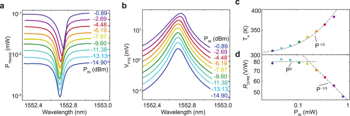
Graphene integrated photonics provides several advantages over conventional Si photonics. Single layer graphene (SLG) enables fast, broadband, and energy-efficient electro-optic modulators, optical switches and photodetectors (GPDs), and is compatible with any optical waveguide. The last major barrier to SLG-based optical receivers lies in the current GPDs' low responsivity when compared to conventional PDs. Here we overcome this by integrating a photo-thermoelectric GPD with a Si microring resonator. Under critical coupling, we achieve >90% light absorption in a ~6 μm SLG channel along a Si waveguide. Cavity-enhanced light-matter interactions cause carriers in SLG to reach ~400 K for an input power ~0.6 mW, resulting in a voltage responsivity ~90 V/W, with a receiver sensitivity enabling our GPDs to operate at a 10-9 bit-error rate, on par with mature semiconductor technology, but with a natural generation of a voltage, rather than a current, thus removing the need for transimpedance amplification, with a reduction of energy-per-bit, cost, and foot-print.


Conflict of interest statement

The authors declare no competing interests.

Figures

Fig. 1
Fig. 1. Si ring resonator integrated GPD.
a Sketch of device. b Transmission spectra of a ring cavity with SLG on top, indicating the effects of varying W on ER and Q. For clarity, the spectra are aligned at the resonance wavelength closest to 1553.55 nm. c Corresponding transmission at resonance. The black line is the calculated transmission for κ = 10%. The coloured dots mark the transmission for various loss coefficients.
Fig. 2
Fig. 2. Device fabrication.
a Assembly of hBN/SLG/hBN. b Stack placement on photonic circuit and interface cleaning. c hBN etching in SF6 plasma. d SLG etching in O2 plasma to define channel geometry. e Metallization (Cr/Au) for drain-source contacts. f Al seed layer evaporation and ALD of Al2O3. g Wet transfer of CVD SLG. h Split-gate fabrication. i Metallization (Cr/Au) for gate contacts.
Fig. 3
Fig. 3. LMH characterisation.
a Microscope image of hBN/SLG/hBN on ring resonator. The black dashed line indicates the area over which the Raman map in d is measured. Scale bar, 10 μm. b Raman spectrum measured at the position of the final device. c AFM image of LMH. The yellow dashed line indicates the area of top and bottom hBN. The blue line indicates the SLG area. Scale bar, 10 μm. d Raman map of FWHM(2D). The red box marks the position of the final device in a, c, d.
Fig. 4
Fig. 4. GPD characterisation.
a False-colour SEM image of our GPD, showing Cr/Au contacts (yellow), Si WG (green), contacted hBN/SLG/hBN (blue, dashed line under contacts), and SLG gates (red). Scale bar: 2 μm. b Resistance map demonstrating independent tunability of charge carrier concentration in the SLG channel via VG1 and VG2. c Electrical characterization at homogeneous channel doping (solid lines, measured data; dashed lines, model). d Calculated S based on the electrical data in c. e, f) Resistance vs. inverse carrier concentration for e electron and f hole doping. g Photoresponse at zero bias on resonance (λ = 1555.87 nm). h Frequency response. The 3-dB cutoff frequency, marked by intersecting dashed lines, is ~12 GHz.
Fig. 5
Fig. 5. Wavelength and power dependence.
a Transmitted power for various Pin. b Photovoltage for a fixed gate voltage combination (VG1 = 1 V, VG2 = − 1 V) for various input powers (same color code as for the transmission in a). c Te calculated from the photoresponse in b and S in Fig. 4d. d Power-dependent R[V/W].

References

    1. Atabaki AH, et al. Integrating photonics with silicon nanoelectronics for the next generation of systems on a chip. Nature. 2018;556:349–354. doi: 10.1038/s41586-018-0028-z. - DOI - PubMed
    1. Cheng Q, Bahadori M, Glick M, Rumley S, Bergman K. Recent advances in optical technologies for data centers: a review. Optica. 2018;5:1354–1370. doi: 10.1364/OPTICA.5.001354. - DOI
    1. Subbaraman H, et al. Recent advances in silicon-based passive and active optical interconnects. Opt. Express. 2015;23:2487–2511. doi: 10.1364/OE.23.002487. - DOI - PubMed
    1. Romagnoli M, et al. Graphene-based integrated photonics for next-generation datacom and telecom. Nat. Rev. Mater. 2018;3:392–414. doi: 10.1038/s41578-018-0040-9. - DOI
    1. Bonaccorso F, Sun Z, Hasan T, Ferrari AC. Graphene photonics and optoelectronics. Nat. Photonics. 2010;4:611–622. doi: 10.1038/nphoton.2010.186. - DOI