Avalanche photodetectors with photon trapping structures for biomedical imaging applications
- PMID: 34154145
- PMCID: PMC8237935
- DOI: 10.1364/OE.421857
Avalanche photodetectors with photon trapping structures for biomedical imaging applications
Abstract
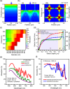
Enhancing photon detection efficiency and time resolution in photodetectors in the entire visible range is critical to improve the image quality of time-of-flight (TOF)-based imaging systems and fluorescence lifetime imaging (FLIM). In this work, we evaluate the gain, detection efficiency, and timing performance of avalanche photodiodes (APD) with photon trapping nanostructures for photons with 450 nm and 850 nm wavelengths. At 850 nm wavelength, our photon trapping avalanche photodiodes showed 30 times higher gain, an increase from 16% to >60% enhanced absorption efficiency, and a 50% reduction in the full width at half maximum (FWHM) pulse response time close to the breakdown voltage. At 450 nm wavelength, the external quantum efficiency increased from 54% to 82%, while the gain was enhanced more than 20-fold. Therefore, silicon APDs with photon trapping structures exhibited a dramatic increase in absorption compared to control devices. Results suggest very thin devices with fast timing properties and high absorption between the near-ultraviolet and the near infrared region can be manufactured for high-speed applications in biomedical imaging. This study paves the way towards obtaining single photon detectors with photon trapping structures with gains above 106 for the entire visible range.
Conflict of interest statement
The authors declare no conflicts of interest.
Figures


References
-
- Hadfield R. H., “Single-photon detectors for optical quantum information applications,” Nat. Photonics 3(12), 696–705 (2009).10.1038/nphoton.2009.230 - DOI
-
- Fan-Yuan G.-J., Teng J., Wang S., Yin Z.-Q., Chen W., He D.-Y., Guo G.-C., Han Z.-F., “Optimizing Single-Photon Avalanche Photodiodes for Dynamic Quantum Key Distribution Networks,” Phys. Rev. Appl. 13(5), 054027 (2020).10.1103/PhysRevApplied.13.054027 - DOI
-
- Zhang C., Lindner S., Antolović I. M., Pavia J. M., Wolf M., Charbon E., “A 30-frames/s, 252 ( 144 SPAD Flash LiDAR With 1728 Dual-Clock 48.8-ps TDCs, and Pixel-Wise Integrated Histogramming,” IEEE J. Solid-State Circuits 54(4), 1137–1151 (2019).10.1109/JSSC.2018.2883720 - DOI
-
- Ximenes A. R., Padmanabhan P., Lee M., Yamashita Y., Yaung D. N., Charbon E., “A 256×256 45/65 nm 3D-stacked SPAD-based direct TOF image sensor for LiDAR applications with optical polar modulation for up to 18.6 dB interference suppression,” in 2018 IEEE International Solid - State Circuits Conference - (ISSCC), 2018), 96–98.

