

Metallization-Induced Quantum Limits of Contact Resistance in Graphene Nanoribbons with One-Dimensional Contacts
- PMID: 34209314
- PMCID: PMC8269807
- DOI: 10.3390/ma14133670
Metallization-Induced Quantum Limits of Contact Resistance in Graphene Nanoribbons with One-Dimensional Contacts
Erratum in
-
Correction: Poljak, M.; Matić, M. Metallization-Induced Quantum Limits of Contact Resistance in Graphene Nanoribbons with One-Dimensional Contacts. Materials 2021, 14, 3670.Materials (Basel). 2021 Nov 18;14(22):6965. doi: 10.3390/ma14226965. Materials (Basel). 2021. PMID: 34832505 Free PMC article.
Abstract
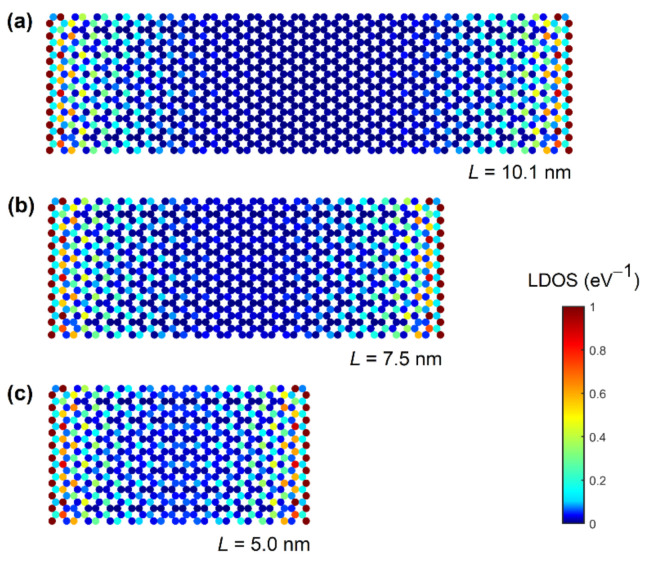
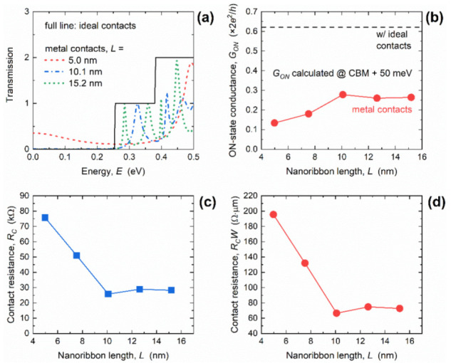
Graphene has attracted a lot of interest as a potential replacement for silicon in future integrated circuits due to its remarkable electronic and transport properties. In order to meet technology requirements for an acceptable bandgap, graphene needs to be patterned into graphene nanoribbons (GNRs), while one-dimensional (1D) edge metal contacts (MCs) are needed to allow for the encapsulation and preservation of the transport properties. While the properties of GNRs with ideal contacts have been studied extensively, little is known about the electronic and transport properties of GNRs with 1D edge MCs, including contact resistance (RC), which is one of the key device parameters. In this work, we employ atomistic quantum transport simulations of GNRs with MCs modeled with the wide-band limit (WBL) approach to explore their metallization effects and contact resistance. By studying density of states (DOS), transmission and conductance, we find that metallization decreases transmission and conductance, and either enlarges or diminishes the transport gap depending on GNR dimensions. We calculate the intrinsic quantum limit of width-normalized RC and find that the limit depends on GNR dimensions, decreasing with width downscaling to ~21 Ω∙µm in 0.4 nm-wide GNRs, and increasing with length downscaling up to ~196 Ω∙µm in 5 nm-long GNRs. We demonstrate that 1D edge contacts and size engineering can be used to tune the RC in GNRs to values lower than those of graphene.
Keywords: NEGF; contact resistance; edge contact; graphene nanoribbon; metallization; one-dimensional contact; quantum transport.
Conflict of interest statement
The authors declare no conflict of interest.
Figures


References
-
- Kuhn K.J. Considerations for Ultimate CMOS Scaling. IEEE Trans. Electron Devices. 2012;59:1813–1828. doi: 10.1109/TED.2012.2193129. - DOI
-
- Takagi S., Takenaka M. III-V/Ge CMOS Technologies on Si Platform; Proceedings of the VLSI Symp; Honolulu, HI, USA. 15–17 June 2010; Piscataway Township, NJ, USA: IEEE; pp. 147–148.
-
- Bolotin K., Sikes K., Jiang Z., Klima M., Fudenberg G., Hone J., Kim P., Stormer H. Ultrahigh electron mobility in suspended graphene. Solid State Commun. 2008;146:351–355. doi: 10.1016/j.ssc.2008.02.024. - DOI
-
- Dorgan V.E., Bae M.-H., Pop E. Mobility and saturation velocity in graphene on SiO2. Appl. Phys. Lett. 2010;97:082112. doi: 10.1063/1.3483130. - DOI
Grants and funding
LinkOut - more resources
Full Text Sources
Miscellaneous
