. 2021 Jul 5;10(1):138.
doi: 10.1038/s41377-021-00577-8.

Ultra-broadband metamaterial absorbers from long to very long infrared regime

Affiliations

Ultra-broadband metamaterial absorbers from long to very long infrared regime

Yu Zhou et al. Light Sci Appl. .

Abstract

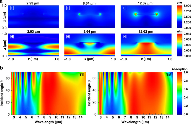
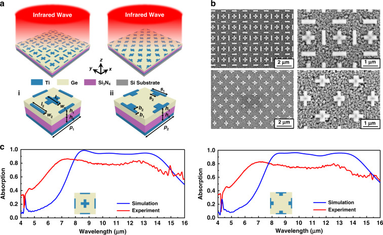
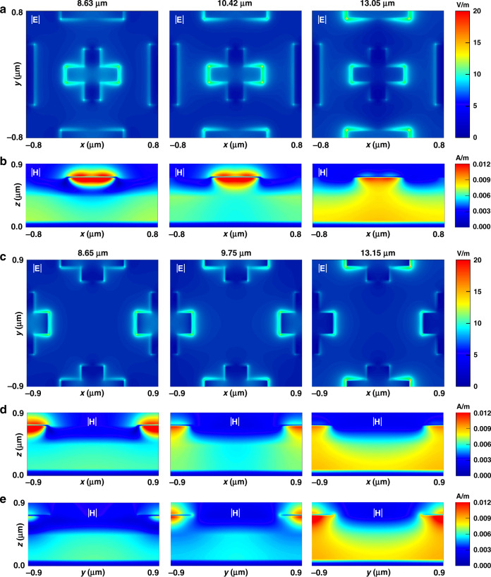
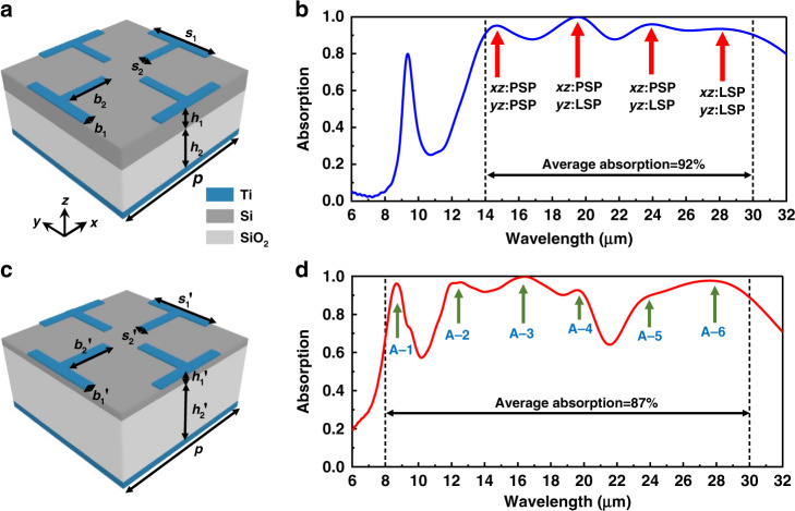
Broadband metamaterials absorbers with high absorption, ultrathin thickness and easy configurations are in great demand for many potential applications. In this paper, we first analyse the coupling resonances in a Ti/Ge/Ti three-layer absorber, which can realise broadband absorption from 8 to 12 μm. Then we experimentally demonstrate two types of absorbers based on the Ti/Ge/Si3N4/Ti configuration. By taking advantage of coupling surface plasmon resonances and intrinsic absorption of lossy material Si3N4, the average absorptions of two types of absorbers achieve almost 95% from 8 to 14 μm (experiment result: 78% from 6.5 to 13.5 μm). In order to expand the absorption bandwidth, we further propose two Ti/Si/SiO2/Ti absorbers which can absorb 92% and 87% of ultra-broadband light in the 14-30 μm and 8-30 μm spectral range, respectively. Our findings establish general and systematic strategies for guiding the design of metamaterial absorbers with excellent broadband absorption and pave the way for enhancing the optical performance in applications of infrared thermal emitters, imaging and photodetectors.


Conflict of interest statement

The authors declare no competing interests.

Figures

Fig. 1
Fig. 1. Absorption characteristics of the Ti/Ge/Ti absorber.
a Schematic of the Ti/Ge/Ti absorber with periodic square top resonators. In this design, l = 0.8 μm, p = 2 μm and h = 0.5 μm. The thickness of the top Ti layer is 22 nm, and the bottom Ti layer is 120 nm, where is thicker than its penetration depth. b SEM images of the fabricated Ti/Ge/Ti absorber. c Schematic of different resonant modes and equivalent RLC circuit of the Ti/Ge/Ti unit cell. d Simulated and experiment absorption spectra of the Ti/Ge/Ti absorber
Fig. 2
Fig. 2. Analyses of electromagnetic field distributions and absorption spectra for different incident angles.
a Electromagnetic field distributions at the three resonant wavelengths along the MIR and LWIR range: 2.93 μm, 8.64 μm and 12.62 μm. b TE-mode (x-polarised) and TM-mode (y-polarised) absorption spectra for incident angles from 0 to 70°
Fig. 3
Fig. 3. Absorption characteristics of two types of Ti/Ge/Si3N4/Ti absorbers.
a Schematic of two types of Ti/Ge/Si3N4/Ti absorbers (h1 = 270 nm, h2 = 330 nm, p1 = 1.6 μm and p2 = 1.8 μm): (i) the top layer consists of periodic nano-cross and nano-strip structures (l1 = 630 nm, w1 = 200 nm, l2 = 750 nm and w2 = 100 nm); (ii) the top layer consists of irregular nano-cross structures (s1 = 850 nm, b1 = 100 nm, s2 = 300 nm and b2 = 200 nm). The thickness of the top Ti layer is 22 nm, and the bottom Ti layer is 120 nm, where is thicker than its penetration depth. b SEM images of two types of fabricated Ti/Ge/Si3N4/Ti absorbers. c Simulated and experiment absorption spectra of the two types of Ti/Ge/Si3N4/Ti absorbers
Fig. 4
Fig. 4. Electromagnetic field distributions of the two types of Ti/Ge/Si3N4/Ti absorbers at their three resonant wavelengths along the LWIR range.
Ti/Ge/Si3N4/Ti absorber with periodic nano-cross and nano-strip top metallic resonators: a electric field distributions in the top layer (x-y plane). b Magnetic field distributions in the dielectric (x-z plane, y = 0). Ti/Ge/Si3N4/Ti absorber with periodic irregular nano-cross top metallic resonators: c electric field distributions in the top layer (x-y plane). d Magnetic field distributions in the dielectric (x-z plane, y = 0). e Magnetic field distributions in the dielectric (y-z plane, x = 0)
Fig. 5
Fig. 5. Simulated absorption characteristics of two types of Ti/Si/SiO2/Ti absorbers from long to very long infrared regime.
a Schematic and b absorption spectrum of the Ti/Si/SiO2/Ti absorber from 14 to 30 μm. (s1 = 1.9 μm, s2 = 0.23 μm, b1 = 0.25 μm, b2 = 1.17 μm, h1 = 0.52 μm, h2 = 1.11 μm and p = 4 μm). c Schematic and d absorption spectrum of the Ti/Si/SiO2/Ti absorber from 8 to 30 μm. (s1′ = 1.9 μm, s2′ = 0.27 μm, b1′ = 0.25 μm, b2′ = 1.21 μm, h1′ = 0.18 μm and h2′ = 1.62 μm) The thickness of the top Ti layer is 22 nm and the bottom Ti layer is 120 nm, which is thicker than its penetration depth

References

    1. Zhang SB, et al. Photonic hyperinterfaces for light manipulations. Optica. 2020;7:687–693. doi: 10.1364/OPTICA.392356. - DOI
    1. Dixon K, et al. Tunable rainbow light trapping in ultrathin resonator arrays. Light Sci. Appl. 2020;9:194. doi: 10.1038/s41377-020-00428-y. - DOI - PMC - PubMed
    1. Zhang XY, et al. Controlling angular dispersions in optical metasurfaces. Light Sci. Appl. 2020;9:76. doi: 10.1038/s41377-020-0313-0. - DOI - PMC - PubMed
    1. Li JY, et al. Inverse design of multifunctional plasmonic metamaterial absorbers for infrared polarimetric imaging. Opt. Express. 2019;27:8375–8386. doi: 10.1364/OE.27.008375. - DOI - PubMed
    1. Li WW, et al. Single-frame wide-field nanoscopy based on ghost imaging via sparsity constraints. Optica. 2019;6:1515–1523. doi: 10.1364/OPTICA.6.001515. - DOI