Review
. 2021 Sep;8(17):e2100864.
doi: 10.1002/advs.202100864. Epub 2021 Jul 13.

Piezoelectric Materials for Energy Harvesting and Sensing Applications: Roadmap for Future Smart Materials

Affiliations
Review

Piezoelectric Materials for Energy Harvesting and Sensing Applications: Roadmap for Future Smart Materials

Susmriti Das Mahapatra et al. Adv Sci (Weinh). 2021 Sep.

Abstract

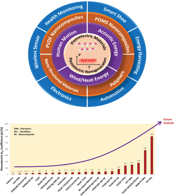
Piezoelectric materials are widely referred to as "smart" materials because they can transduce mechanical pressure acting on them to electrical signals and vice versa. They are extensively utilized in harvesting mechanical energy from vibrations, human motion, mechanical loads, etc., and converting them into electrical energy for low power devices. Piezoelectric transduction offers high scalability, simple device designs, and high-power densities compared to electro-magnetic/static and triboelectric transducers. This review aims to give a holistic overview of recent developments in piezoelectric nanostructured materials, polymers, polymer nanocomposites, and piezoelectric films for implementation in energy harvesting. The progress in fabrication techniques, morphology, piezoelectric properties, energy harvesting performance, and underpinning fundamental mechanisms for each class of materials, including polymer nanocomposites using conducting, non-conducting, and hybrid fillers are discussed. The emergent application horizon of piezoelectric energy harvesters particularly for wireless devices and self-powered sensors is highlighted, and the current challenges and future prospects are critically discussed.

Keywords: energy harvesting; flexible devices; nanostructured materials; piezoelectric nanogenerator; polymer nanocomposites; polyvinylidene fluoride copolymers.


Conflict of interest statement

The authors declare no conflict of interest.

Figures

Figure 1
Figure 1
Operating modes of a piezoelectric material a) 33 mode and b) 31 mode.
Figure 2
Figure 2
Schematic of 2 D crystal structures. a) Non‐piezoelectric square. b) Piezoelectric hexagon.
Figure 3
Figure 3
Schematic diagram showing the poling systems. a) Electrode poling. b) Corona poling.
Figure 4
Figure 4
Diagram showing the working mechanism of an energy harvester. Reproduced with permission.[ 64 ] Copyright 2016, American Chemical Society.
Figure 5
Figure 5
Schematic diagram of the PENG and FE‐SEM image of ZnO NR arrays grown on ITO coated PES substrate (scale bar: 300 nm). Reproduced with permission.[ 84 ] Copyright 2009, Wiley‐VCH.
Figure 6
Figure 6
a) Experimental setup for transferring vertically grown ZnO NWs to a flexible substrate to make horizontally aligned ZnO NW arrays. b) SEM image of vertically aligned ZnO NWs grown on Si substrate by a physical vapor deposition method. c) SEM image of the as‐transferred horizontal ZnO NWs on a flexible substrate. d) V oc and e) I sc measured from the PENG at a strain of 0.1% and a strain rate of 5% s–1 with a deformation frequency of 0.33 Hz. The insets are an enlarged view of the boxed area for one cycle of deformation. Reproduced with permission.[ 50 ] Copyright 2010, American Chemical Society.
Figure 7
Figure 7
a) Schematic diagram of the textile‐based hybrid NG. b,c) Large‐area SEM images of ZnO NWs grown on textile substrate. d) Photographic image of textile substrate post rolling. Adapted with permission.[ 98 ] Copyright 2012, The Royal Society of Chemistry.
Figure 8
Figure 8
a) FE‐SEM image of the ZnO nanosheets network grown on Al. b) Schematic image of 2D ZnO nanosheet‐based NG. c) Output voltage and current density of the NG obtained by varying the applied pushing force. Reproduced with permission.[ 106 ] Copyright 2013, Springer Nature.
Figure 9
Figure 9
a) Schematic of the PZT nanofiber NG, b) SEM image of the electrospun PZT nanofibers. c) Cross‐sectional SEM image of the PZT nanofibers embedded in PDMS matrix. Reproduced with permission.[ 118 ] Copyright 2010, American Chemical Society.
Figure 10
Figure 10
a) The fabrication process of the NG using oriented electrospun nanofibers. b) The output voltage of the NG under a periodic pressure of 0.53 MPa. a,b) Reproduced with permission.[ 120 ] Copyright 2012, American Chemical Society. c) SEM image showing the hetero‐junction structure of ZnO NWs/PZT. Reproduced with permission.[ 122 ] Copyright 2013, Elsevier B.V. d) SEM image of PMN‐PT nanowires. Reproduced with permission.[ 123 ] Copyright 2012, American Chemical Society.
Figure 11
Figure 11
a) Cross‐sectional SEM image of the as‐synthesized BaTiO3 NW arrays with inset showing the top view. b) Schematic of the energy harvester constructed using BaTiO3 NW arrays. c) Power and d) power density of the BaTiO3 NW based PEH at various load resistances displaying a peak power of ≈125.5 pW and a peak power density of ≈6.27 µW cm–3 at an optimal resistance of 120 MΩ from 1 g acceleration. These peak power levels are much greater than the peak power from ZnO NW based PEH. Reproduced with permission.[ 126 ] Copyright 2014, The Royal Society of Chemistry.
Figure 12
Figure 12
Schematic representation of the chain conformation for the α, β, and γ phases of PVDF. Reproduced with permission.[ 150 ] Copyright 2014, Elsevier Ltd.
Figure 13
Figure 13
a) Near‐field electrospinning (NFES) to create PVDF nanofibers onto a substrate. b) Output voltage and c) current measured with respect to time under applied strain at 2 Hz. a‐c) Reproduced with permission.[ 201 ] Copyright 2010, American Chemical Society. d) Schematic depiction of PVDF nano porous arrays grown by the template‐assisted method. e) Piezoelectric potential and f) current obtained from porous PVDF and bulk films under the same force. d‐f) Reproduced with permission.[ 208 ] Copyright 2011, American Chemical Society. g) Schematic diagram of mesoporous PVDF film. h) The voltage and i) current output of the PENG under perpetual surface oscillation. Insets show the output curve in the course of one oscillation cycle. g‐i) Reproduced with permission.[ 209 ] Copyright 2014, Wiley‐VCH.
Figure 14
Figure 14
Schematic representation of the a) P(VDF‐TrFE), b) P(VDF‐HFP), and c) P(VDF‐CTFE) repeat units. Reproduced with permission.[ 150 ] Copyright 2014, Elsevier Ltd.
Figure 15
Figure 15
a) Schematic diagram of the PENG, showing the nanocomposite film consisting of BaTiO3 clusters. b) Rectified V oc of the PENG with a full‐wave rectifier under periodic finger impartation. The inset is an enlarged view of a voltage pulse in the dashed line. a,b) Reproduced with permission.[ 270 ] Copyright 2014, American Chemical Society. c) Schematic of the proposed process leading to increased β‐phase content in PVDF due to BaTiO3 filler addition. Reproduced with permission.[ 271 ] Copyright 2017, American Chemical Society.
Figure 16
Figure 16
Schematic diagram showing a) BaTiO3 NPs showing aggregation in PVDF matrix; inset showing the formation of β phase on BaTiO3 NPs. b) Pdop‐BaTiO3 showing good dispersion on the surface of electrospun P(VDF‐TrFE) fiber; inset displaying the interfacial interactions between BaTiO3, Pdop, and P(VDF‐TrFE). Reproduced with permission.[ 280 ] Copyright 2020, Elsevier Ltd.
Figure 17
Figure 17
a) Crystalline structure diagram of BaTi2O5 with the A2/m spacing group. The 5 vol% BT2/PVDF PENG showing b) stability and durability under vibration condition and c) voltage generation by the beating of bicycle spokes. Reproduced with permission.[ 254 ] Copyright 2018, Elsevier Ltd.
Figure 18
Figure 18
a) Schematic diagram of the fabricated PENG. b) Photograph of attachment of the PENG on the hand. c,d) Output voltage and current under the touching condition of the device on hand. e) Snapshot of the lighting of blue LEDs driven using PENG under periodic finger impartation. Reproduced with permission.[ 293 ] Copyright 2018, Elsevier Ltd.
Figure 19
Figure 19
a) SEM images of undoped ZnO and b) Co‐doped ZnO nanorods. a,b) Reproduced with permission.[ 296 ] Copyright 2018, Springer Nature. c) TEM image of Fe‐doped ZnO particles. Reproduced with permission.[ 298 ] Copyright 2018, The Royal Society of Chemistry. d) Sample flexibility and schematic of bending experiment. e) Interaction mechanism in the nanocomposites consisting of dual layers of P(VDF‐HFP)/Fe‐ZnO and P(VDF‐HFP)/CNC. Reproduced with permission.[ 299 ] Copyright 2019, Elsevier Ltd.
Figure 20
Figure 20
a) Output voltage performance of PVDF/ZF(PEG)‐12 wt% nanocomposites. b) Impact sensing capability of the nanocomposites. c) Proposed interactions of untreated and surface‐treated zinc ferrite with PVDF. Reproduced with permission.[ 303 ] Copyright 2017, Elsevier B.V.
Figure 21
Figure 21
a) Schematic diagram showing hydrogen bond formation in P(VDF‐TrFE)/MgO nanocomposites. b) Voltage generated by the 2 wt% MgO/P(VDF‐TrFE) nanocomposite‐based PENG on continuous finger tapping. c) Variation of d33 coefficient as a function of bending cycles at different strain rates. Reproduced with permission.[ 319 ] Copyright 2017, American Chemical Society.
Figure 22
Figure 22
a) SEM micrograph of the electrospun 0.50 wt% talc/PVDF composite nanofibers. b) The output voltage of the PENG obtained by continuous finger tapping using PVDF and talc/PVDF nanocomposite fibers. c) Proposed mechanism of interactions between talc nanosheets and PVDF chains in the electrospun nanofibers. Reproduced with permission.[ 333 ] Copyright 2020, The Royal Society of Chemistry.
Figure 23
Figure 23
The piezoelectric response of a) P(VDF‐TrFE) nanocomposites with Ag NPs and Ag NWs. b) P(VDF‐TrFE)/Ag NWs nanocomposites with various loadings of Ag NWs (35 nm in diameter). c) Schematic of crystal structure on Ag NW surface. d) Arrangement of P(VDF‐TrFE) chains absorbed on Ag NP surface. Reproduced with permission.[ 339 ] Copyright 2016, Elsevier B.V.
Figure 24
Figure 24
a) Schematic demonstration of the electrospinning setup. b) Outstanding flexibility illustration of Pt/PVDF nanofibers mat by rolling around an irregular object. c) Photograph of the flexible PENG with d) 3D design showing e) SEM image of aligned arrays of Pt/PVDF nanofibers along the surface direction with their polarization direction along the thickness direction. f) Interlocking micro‐fiber arrays of conducting fabric. Reproduced with permission.[ 342 ] Copyright 2018, Elsevier Ltd.
Figure 25
Figure 25
Schematic image showing the proposed mechanism of chain extension in PVDF induced by electrospinning and mechanical drawing. Reproduced with permission.[ 337 ] Copyright 2013, American Chemical Society.
Figure 26
Figure 26
a) Schematic diagram of MWCNTs functionalization by ionic liquid to form MWCNT‐IL. TEM images of b) pristine MWCNTs and c) IL‐functionalized MCWNTs. Reproduced with permission.[ 349 ] Copyright 2013, American Chemical Society.
Figure 27
Figure 27
Schematic reflecting the role of CNTs on β phase formation in PVDF. a) The chemical bonding between functionalized CNTs and PVDF chains. b) The adsorbed PVDF chains on the CNT surface influenced by the dispersion of CNTs. Reproduced with permission.[ 350 ] Copyright 2013, Elsevier Ltd.
Figure 28
Figure 28
SAXS patterns of a) solution cast, b) rolled pure PVDF (inset) and composites with 0.7 wt% TiO2@MWCNTs loading. TEM images of c) solution cast and d) rolled composites with 0.7 wt% loading, wherein the arrow points to the rolling direction. The inset in (c) represents the TEM image of the solution cast pure PVDF. Reproduced with permission.[ 354 ] Copyright 2016, Elsevier Ltd.
Figure 29
Figure 29
a) FE‐SEM image of PVDF/Ce‐graphene nanofibers. The inset shows the statistical size distribution of the NFs. b) TEM image and higher‐resolution image (inset) of PVDF/Ce‐graphene NFs. c) The output voltage from the PENG driven by the music of 88 dB intensity. Instantaneous lighting of 3 blue LEDs shown in the inset. d) Voltages from various instruments‐flute, guitar and violin of the National anthem of India. Reproduced with permission.[ 361 ] Copyright 2016, American Chemical Society.
Figure 30
Figure 30
a) Output voltage and current are shown as a function of Fe‐rGO filler loading in PVDF. b) Proposed schematic showing the interactions between γ‐phase in PVDF and a Fe‐rGO nanosheet (by assuming a single γ‐phase and Fe‐RGO sheet). Reproduced with permission.[ 368 ] Copyright 2015, The Royal Society of Chemistry.
Figure 31
Figure 31
a) The mechanism of PVDF/rGO‐ZnO nanocomposite films production. Reproduced with permission.[ 370 ] Copyright 2014, Elsevier B.V. b) Output voltage and c) current generated from 1 wt% AlO‐rGO/PVDF PENG. b,c) Reproduced with permission.[ 371 ] Copyright 2016, Wiley‐VCH.
Figure 32
Figure 32
Cross‐sectional SEM image of a) CB‐0.5/P(VDF‐HFP) composite film b) CB‐0.5FLG‐0.03 composite film. The particles circled in (a) and (b) shows the nanofillers. Harvested power density of c) 0.3 wt% CB and different FLG loadings. d) 0.5 wt% CB and different FLG loadings. Reproduced with permission.[ 265 ] Copyright 2019, Elsevier Ltd.
Figure 33
Figure 33
a) Schematic diagram of the fabricated PENG device. The inset is a cross‐sectional SEM image of the PENG. b) V oc measurements of the PENG in transverse (d33) mode with a magnified view of the selected region. The inset in the magnified view illustrates the d33 mode generator. Reproduced with permission.[ 381 ] Copyright 2018, Elsevier B.V.
Figure 34
Figure 34
a) The synthesis route of the MWCNTs/graphene/MnO2 hybrid. SEM, TEM, and high‐resolution TEM images of b–d) CM23 and e–g) CM66 hybrids. h) Variation of piezoelectric coefficients d33 with poling electric fields in CM23 and CM66 nanocomposites. Reproduced with permission.[ 268 ] Copyright 2018, Elsevier Ltd.
Figure 35
Figure 35
a) Schematic illustration of overall fabrication for BaTiO3 NWs‐based PENG. b) Photograph of the PENG (3 cm × 4 cm) completely bent by human fingers. The inset shows the nanocomposite layer stretched by fingers without any damage. c) The electrical signals measured from the PENG. Reproduced with permission.[ 392 ] Copyright 2014, The Royal Society of Chemistry.
Figure 36
Figure 36
a) Fabrication of piezoelectric BaTiO3 nanocube/PDMS composite films using solution casting technique. The inset photographs show the transparency of the composites with various weight ratios of BaTiO3 NCs in the PDMS matrix. b,c) Photographs demonstrating the flexibility and rolling capabilities of the nanocomposite films. d) Schematic diagram of the PENG for harnessing mechanical energy. e) Comparison of JV responses of the PENG as a function of BaTiO3 nanocube weight ratio under low mechanical pressure of 988.14 Pa. Reproduced with permission.[ 396 ] Copyright 2017, American Chemical Society.
Figure 37
Figure 37
a) Schematic diagram of the fabrication process for stretchable composites embedded with hemispheres. b) Output voltage and c) current density generated by the composites embedded with ZnO hemispheres as a function of the diameter of the hemispheres from 0.5 to10 µm and PZT hemispheres of 10 µm under convex bending strain. Reproduced with permission.[ 402 ] Copyright 2014, Elsevier Ltd.
Figure 38
Figure 38
a) SEM image of the as‐fabricated CNF aerogel. b) Schematic diagram of the flexible porous CNF/PDMS aerogel film‐based PENG. c) Cross‐sectional SEM image of the PENG at high magnification. d) Output voltage generated from the PENG. Reproduced with permission.[ 405 ] Copyright 2016, Elsevier Ltd.
Figure 39
Figure 39
The output voltage, current, and power of PENGs generated under periodic mechanical compression of 2 kPa with a) 30 wt% BaTiO3 nanofibers and different MWCNT contents (0–5 wt%), b) 2.0 wt% MWCNT, and different BaTiO3 nanofiber contents (10–50 wt%). Cross‐sectional SEM images of PENGs with c) 2.0 wt% MWCNTs and 30 wt% BaTiO3 nanofibers, d) 2.0 wt% MWCNTs, and 40 wt% BaTiO3 nanofibers. Reproduced with permission.[ 412 ] Copyright 2017, Elsevier Ltd.
Figure 40
Figure 40
a) Schematic diagram of the hyper‐stretchable PENG based on PMN‐PT/MWCNT composite and Ag NWs stretchable electrodes. b) The PENG device stretched by human hands. Inset showing PENG is released again without damage. c) SEM image showing well‐distributed PMN‐PT particles and MWCNTs in the silicone rubber matrix. d–f) Photographs of the PENG when subjected to various deformations, such as twisting, folding, and crumpling. g) These motions are converted to a corresponding voltage. Reproduced with permission.[ 416 ] Copyright 2015, Wiley‐VCH.
Figure 41
Figure 41
FESEM images of a) pure PVDF, b) ErCl3.6H2O/PVDF films with 5 wt% Er, c) Fe(NO3)3·9H2O/PVDF films with 10 wt% Fe. d) Schematic of the PENG device. Open circuit voltage (V oc) generated by the PENGs containing e) 5 wt% Er3+/PVDF and f) 10 wt% Fe3+/PVDF composites. Reproduced with permission.[ 420 ] Copyright 2017, American Chemical Society.
Figure 42
Figure 42
a) Schematic diagram of the fabrication process for PZT thin film‐based PENG via LLO method. Cross‐sectional SEM images of PZT thin films on b) Al2O3 and c) PET substrate. d) V oc and cross‐sectional current density measured from the PENG. a‐d) Reproduced with permission.[ 428 ] Copyright 2014, Wiley‐VCH. e) Schematic of the bilayer films PEH. f) Photograph showing that the PEH is freestanding, flexible, bendable, and rollable. g) The voltage output from the PEH. e‐g) Reproduced with permission.[ 429 ] Copyright 2015, American Chemical Society.
Figure 43
Figure 43
a) Optical image of the PENG under finger pressing. b) Output voltage generated from the PENG by finger pressing‐releasing process. c) A commercial electric watch and 15 LEDs driven by the PENG. The optical images and output voltages generated by human motions of d) wrist flexing, e) finger taping, and foot stepping by f) heel and g) toe. Reproduced with permission.[ 433 ] Copyright 2018, Elsevier Ltd.
Figure 44
Figure 44
a–c) Schematic and photographic images of different vehicles such as bicycle, motorcycle, and car passing on the Ag/BaTiO3‐PENG device. d–f) The corresponding output voltage from the PENG. Reproduced with permission.[ 439 ] Copyright 2018, Elsevier Ltd.
Figure 45
Figure 45
a,b) V oc and I sc generated by PENG at water velocities of 31.43, 78.6, and 125.7 ms–1. The insets of (a,b) show output generated under water ON and OFF conditions. Reproduced with permission.[ 434 ] Copyright 2015, American Chemical Society.
Figure 46
Figure 46
a) Photographs of the pressure sensor attached to a shoe insole. b–d) Schematic diagrams and the output currents produced by squatting up and down, walking, and running. e) Output currents with elbow flexion and extension for 60°, 90°, and 120°. Reproduced with permission.[ 438 ] Copyright 2018, The Royal Society of Chemistry.
Figure 47
Figure 47
a) Demonstration of the self‐powered device consisting of a ZnO microwire pH sensor and a composite nanogenerator. b) Electrical output as a function of pH across the pH sensor. The inset shows the voltage as a function of different pH values. Reproduced with permission.[ 435 ] Copyright 2014, American Chemical Society.
Figure 48
Figure 48
a) PENG affixed to the skin near a human eye for detecting wrinkling of the face. b) Output signal recorded while blinking of an eye. Reproduced with permission.[ 23 ] Copyright 2014, Elsevier Ltd.
Figure 49
Figure 49
a) Schematic showing the various energy sources from which piezoelectric power is generated, the different piezoelectric materials, PENGs and their fabrication techniques and the various applications in the center. b) The plot of piezoelectric coefficients (d33) of various materials. The arrow points toward future outlook suggesting that a material with higher d33 than 600 pC N–1 needs to be developed to meet the piezoelectric requirements of the future.

References

    1. Brown T. W., Bischof‐Niemz T., Blok K., Breyer C., Lund H., Mathiesen B. V., Renewable Sustainable Energy Rev. 2018, 92, 834.
    1. Paradiso J. A., Starner T., IEEE Pervasive Comput. 2005, 4, 18.
    1. Wei C., Jing X., Renewable Sustainable Energy Rev. 2017, 74, 1.
    1. Dewan A., Ay S. U., Karim M. N., Beyenal H., J. Power Sources 2014, 245, 129.
    1. Selvan K. V., Ali M. S. M., Renewable Sustainable Energy Rev. 2016, 54, 1035.

Publication types

Substances

LinkOut - more resources