. 2021 Jul 20;12(1):4421.
doi: 10.1038/s41467-021-24494-x.

Room-temperature control and electrical readout of individual nitrogen-vacancy nuclear spins

Affiliations

Room-temperature control and electrical readout of individual nitrogen-vacancy nuclear spins

Michal Gulka et al. Nat Commun. .

Abstract

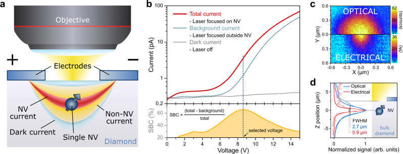
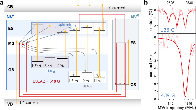
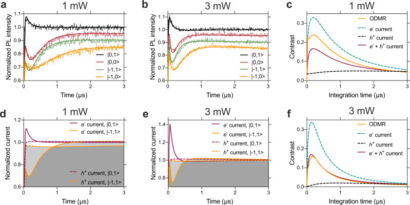
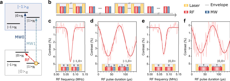
Nuclear spins in semiconductors are leading candidates for future quantum technologies, including quantum computation, communication, and sensing. Nuclear spins in diamond are particularly attractive due to their long coherence time. With the nitrogen-vacancy (NV) centre, such nuclear qubits benefit from an auxiliary electronic qubit, which, at cryogenic temperatures, enables probabilistic entanglement mediated optically by photonic links. Here, we demonstrate a concept of a microelectronic quantum device at ambient conditions using diamond as wide bandgap semiconductor. The basic quantum processor unit - a single 14N nuclear spin coupled to the NV electron - is read photoelectrically and thus operates in a manner compatible with nanoscale electronics. The underlying theory provides the key ingredients for photoelectric quantum gate operations and readout of nuclear qubit registers. This demonstration is, therefore, a step towards diamond quantum devices with a readout area limited by inter-electrode distance rather than by the diffraction limit. Such scalability could enable the development of electronic quantum processors based on the dipolar interaction of spin-qubits placed at nanoscopic proximity.


Conflict of interest statement

The authors declare no competing interests.

Figures

Fig. 1
Fig. 1. Electrical detection of single NV centre.
a Schematic of the PDMR chip with the single NV centre used for the measurements. A yellow-green 561 nm laser is focused between the contacts (with an inter-electrode distance of 3.5 µm) using a microscope objective in air (N.A. = 0.95). The resulting currents are measured versus the bias voltage applied to the electrodes. We identify three types of currents: dark current—not related to the laser illumination, non-NV photocurrent—laser-induced photocurrent not originating from the NV centre, NV photocurrent—current from the two-photon ionization of the single NV centre. b Current–voltage characteristic curves for laser off (grey, dark current), for laser (4 mW) focused away from the single NV centre (cyan, background current from dark current and non-NV photocurrent) and for laser (4 mW) focused on the single NV centre (red, total current from dark current, non-NV photocurrent, and NV photocurrent). The bias voltage for the photocurrent measurements was set to 8.6 V as determined from the maximum signal-to-background contrast (SBC) calculated from the background and total current (dark yellow). c, d Simultaneous optical and electrical imaging of the single NV centre (laser power 6 mW). c XY map showing the size comparison of the same NV centre for the two detection methods. d Z scan of the NV. Darker curves are the Lorentzian fits of the experimental data points, FWHM stands for full width at half maximum calculated from the fitted data.
Fig. 2
Fig. 2. PDMR detection at ESLAC.
a Schematic describing the photoelectric readout principle at ESLAC. Only transitions responsible for the PDMR contrast between the different electron and nuclear spin states are visualized. The |ms〉 = |+1〉 state, which was not probed in these experiments, is omitted for clarity. Under the application of the magnetic field (~510 G for ESLAC), the NV centre ground state (GS) energy levels |ms〉 = |−1〉 and |ms〉 = |0〉 are well separated (~1.5 GHz), whereas the excited state (ES) becomes nearly degenerate resulting in spin mixing between the states with the equivalent total spin projection quantum number. The spin mixing combined with the electron spin polarisation to |ms〉 = |0〉 through the metastable state (MS) [grey arrows], results in the spin polarisation to the |ms〉 = |0〉 electron and |mI〉 = |+1〉 nuclear spin state. The yellow arrows depict optical transitions induced by the application of the yellow-green laser. As can be seen, the |ms〉 = |0〉 spin sublevels in the ES are more likely to be excited by the second photon and contribute to the photocurrent by promoting the NV electron to the diamond conduction band (CB). When this happens, the negatively charged NV centre is converted to NV0 centre (red arrows). The back-conversion is possible by another two-photon process while preserving the nuclear spin orientation. First, the NV0 centre is excited to the ES and subsequently, an electron is promoted from the valence band (VB) to the vacated orbital of NV0, leading to the formation of NV centre. In this process the NV |ms〉 = |0〉 ground states efficiently repolarise. b Pulsed PDMR measurements of the NV nuclear (14N) and electron (ms = −1) spin hyperfine interaction for different magnetic fields showing nuclear spin polarisation close to the ESLAC (experimental conditions for measurement at 123 G—1500 ns laser pulse of 4 mW power, 1100 ns long MW π-pulse; for measurement at 439 G—1000 ns laser pulse of 6 mW power, 400 ns long MW π-pulse).
Fig. 3
Fig. 3. Photon and charge carrier emission dynamics and intrinsic spin contrast.
a, b The experimental (thin) and theoretical (bold) time traces of the normalized PL intensity upon turning on the laser excitation pulse of 1 and 3 mW power, respectively, for various initial electron and nuclear spin states. For a better visibility, the curves corresponding to |0,0〉, |−1,1〉 and |−1,0〉 initial states are shifted down by 0.05, 0.1 and 0.15, respectively. To prepare different initial spin states in the experiment, RF, MW0 and MW1 π-pulses were used (see Fig. 4a). The theoretical results closely follow the experimental curves. d, e The time traces of the simulated electron currents (solid lines) and hole currents (dashed lines) for 1 and 3 mW laser power, respectively, for |0,1〉 and |−1,1〉 initial spin states. The curves are normalized to the steady-state electron current obtained for the |0,1〉 initial spin state. The areas below the electron and hole currents (grey areas under the solid and dashed lines) are integrated to the same value to ensure the charge neutrality constraint of the photoionization cycle. The difference between the solid (dashed) curves provides the spin contrast of the electron (hole) current. c, f The theoretical ODMR contrast and the contrast of the electron-only current, the hole-only current, and the total current (PDMR) as a function of integration time for 1 and 3 mW excitation power, respectively. In the case of ODMR and PDMR, the contribution of the experimental background signal is taken into consideration as well.
Fig. 4
Fig. 4. Electrical readout of individual nuclear spin.
a Schematic of the NV ground state hyperfine energy-level structure of the |ms〉 = |0〉 and |ms〉 = |−1〉 states depicting the resonant frequencies of the probed transitions (RF: radiofrequency, MW0: resonant microwave frequency to selectively excite the electron spin in |mI〉 = |0〉, MW1: resonant microwave frequency to selectively excite the electron spin in |mI〉 = |+1〉). b Scheme of the envelope pulse train designed for electrical readout of a single nuclear spin using the lock-in detection technique. Here, the lock-in amplifier is triggered by the on/off envelope modulation of the laser pulses. c Electrically-detected RF resonant frequency of the |0,+1〉 and |0,0〉 transitions of the single 14N nuclear spin measured at 439 G. Inset shows the pulse sequence used, consisting of RF and MW0 π-pulses. d Corresponding electrically-detected Rabi oscillations of the single nuclear spin with the pulse sequence shown in the inset. e Electrically-detected RF resonant frequency of the |0,+1〉 and |0,0〉 transitions of the single 14N nuclear spin without electron spin manipulation measured at 439 G. Inset shows the pulse sequence used consisting of RF π-pulses. f Corresponding electrically-detected Rabi oscillations of the single nuclear spin with the pulse sequence shown in the inset (experimental conditions: 4000 ns laser pulse of 6 mW power, 400 ns long MW π-pulse, 1 W RF power).

References

    1. Ladd TD, et al. Quantum computers. Nature. 2010;464:45–53. doi: 10.1038/nature08812. - DOI - PubMed
    1. Chuang IL, Vandersypen LMK, Zhou X, Leung DW, Lloyd S. Experimental realization of a quantum algorithm. Nature. 1998;393:143–146. doi: 10.1038/30181. - DOI
    1. Li Z, et al. Experimental realization of a compressed quantum simulation of a 32-spin Ising chain. Phys. Rev. Lett. 2014;112:220501. doi: 10.1103/PhysRevLett.112.220501. - DOI - PubMed
    1. Childress L, et al. Coherent dynamics of coupled electron and nuclear spin qubits in diamond. Science. 2006;314:281–285. doi: 10.1126/science.1131871. - DOI - PubMed
    1. Neumann P, et al. Multipartite entanglement among single spins in diamond. Science. 2008;320:1326–1329. doi: 10.1126/science.1157233. - DOI - PubMed