. 2021 Jul 23;7(30):eabh0863.
doi: 10.1126/sciadv.abh0863. Print 2021 Jul.

Layer-engineered interlayer excitons

Affiliations

Layer-engineered interlayer excitons

Qinghai Tan et al. Sci Adv. .

Abstract

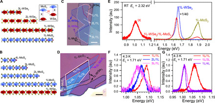
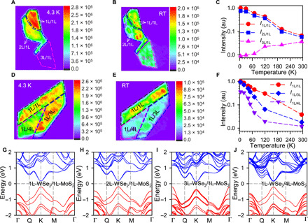
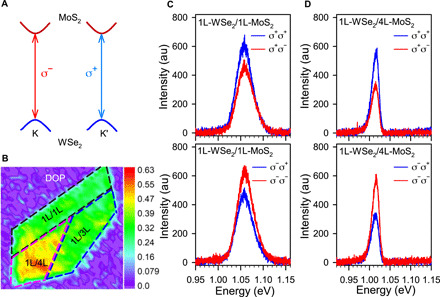
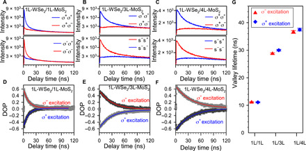
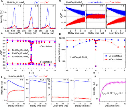
Photoluminescence (PL) from excitons serves as a powerful tool to characterize the optoelectronic property and band structure of semiconductors, especially for atomically thin two-dimensional transition metal dichalcogenide (TMD) materials. However, PL quenches quickly when the thickness of TMD materials increases from monolayer to a few layers, due to the change from direct to indirect band transition. Here, we show that PL can be recovered by engineering multilayer heterostructures, with the band transition reserved to be a direct type. We report emission from layer-engineered interlayer excitons from these multilayer heterostructures. Moreover, as desired for valleytronics devices, the lifetime, valley polarization, and valley lifetime of the generated interlayer excitons can all be substantially improved as compared with that in the monolayer-monolayer heterostructure. Our results pave the way for controlling the properties of interlayer excitons by layer engineering.


Figures

Fig. 1
Fig. 1. Observation of IXs in mL-WSe2/1L-MoS2 and 1L-WSe2/mL-MoS2 heterostructures.
(A and B) A schematic of the IXs in mL-WSe2/1L-MoS2 and 1L-WSe2/mL-MoS2 heterostructures (HS), respectively. The inset shows a type II band alignment of WSe2/MoS2 heterostructure [intralayer exciton (X); interlayer exciton (IX)]. For IX, the electrons and holes are separated in MoS2 and WSe2 layers, respectively. (C and D) The optical microscope image of the mL-WSe2/1L MoS2 (labeled as mL/1L; m = 1 to 3) sample (S1) and 1L-WSe2/mL-MoS2 (labeled as 1L/mL; m = 1, 3, and 4) sample (S2). WSe2 and MoS2 with different layers are marked with dashed lines of different colors. The heterostructure regions are marked with solid white lines. Scale bars, 10 μm. (E) The PL spectra of intralayer excitons in monolayer WSe2 and MoS2 and IXs in 1L-WSe2/1L-MoS2 heterostructure sample at room temperature (RT). (F and G) The PL spectra of IXs in mL-WSe2/1L-MoS2 heterostructure and 1L-WSe2/mL-MoS2 heterostructure at low temperature. au, arbitrary units.
Fig. 2
Fig. 2. Temperature dependence of IXs in mL-WSe2/1L-MoS2 and 1L-WSe2/mL-MoS2 heterostructures.
(A and B) The PL intensity map of the IXs in mL-WSe2/1L-MoS2 (mL/1L; m = 1 to 3) HS at 4.3 K and room temperature, respectively. (C) The PL intensity of IXs in mL-WSe2/1L-MoS2 as a function of temperature. The PL intensity is the average values of multiple positions of each mL-WSe2/1L-MoS2 region. (D and E) The PL intensity map of the IXs in 1L-WSe2/mL-MoS2 (mL/1L; m = 1, 3, and 4) HS at 4.3 K and room temperature, respectively. A 1064-nm long pass was used to ensure that only the IX signal can be detected. (F) The PL intensity of IXs in 1L-WSe2/mL-MoS2 as a function of temperature. The PL intensity is the average values of multiple positions of each 1L-WSe2/mL-MoS2 region. (G to J) The calculated electronic energy structure of 1L-WSe2/1L-MoS2, 2L-WSe2/1L-MoS2, 3L-WSe2/1L-MoS2, and 1L-WSe2/4L-MoS2 heterostructures, respectively.
Fig. 3
Fig. 3. Circularly polarized PL spectra of IXs in 1L-WSe2/mL-MoS2 heterostructures.
(A) A simplified schematic of valley optical selection rule for IXs in K and K′ valley. The electrons and holes are located at K (K′) point of the MoS2 conduction band and WSe2 valence band, respectively. (B) The valley DOP mapping of IXs in the multilayer HS calculated from the polarized PL intensity mapping measurement results. (C and D) The circularly polarized PL spectra of IXs from 1L-WSe2/1L-MoS2 and 1L-WSe2/4L-MoS2 heterostructure regions, respectively. σiσj represents excitation with σi and detection with σj circular polarization.
Fig. 4
Fig. 4. Layer-engineered depolarization lifetime of IX in 1L-WSe2/mL-MoS2 heterostructures.
(A to C) Time-resolved circularly polarized PL of IXs from 1L-WSe2/1L-MoS2, 1L-WSe2/3L-MoS2, and 1L-WSe2/4L-MoS2 HS regions, respectively. The IX lifetime of a few hundred nanoseconds was observed. The temperature for PL decay measurements is 4.3 K. (D to F) The time-resolved valley DOP of IXs obtained from the measured time-resolved circularly polarized PL in (A) to (C). (G) The valley DOP lifetimes under left and right circularly polarized light excitation.
Fig. 5
Fig. 5. Suppression of valley relaxation under magnetic field for IXs in 1L-WSe2/mL-MoS2 heterostructures.
(A) Valley polarization for IXs in 1L-WSe2/4L-MoS2 under three magnetic fields: −1, 0, and 1 T. An enhanced valley polarization under magnetic field has been observed. (B) Magnetic dependence of DOP. Valley mixing has been suppressed for all m = 1, 3, and 4 cases. (C) Time-resolved DOP for IXs in 1L-WSe2/4L-MoS2 at −1, 0, and 1 T (0.125-MHz repetition rate is used here). An enhanced valley polarization lifetime has been observed under magnetic field. (D) The magnetic field dependence of valley DOP lifetime under left and right circularly polarized light excitation, respectively. (E) Time-resolved photon emission at different magnetic fields. (F) The magnetic field suppressed valley relaxation characterization. The temperature for all measurements under magnetic fields is around 4.3 K.

References

    1. Wang G., Chernikov A., Glazov M. M., Heinz T. F., Marie X., Amand T., Urbaszek B., Colloquium: Excitons in atomically thin transition metal dichalcogenides. Rev. Mod. Phys. 90, 021001 (2018).
    1. Splendiani A., Sun L., Zhang Y., Li T., Kim J., Chim C.-Y., Galli G., Wang F., Emerging photoluminescence in monolayer MoS2. Nano Lett. 10, 1271–1275 (2010). - PubMed
    1. Mak K. F., Lee C., Hone J., Shan J., Heinz T. F., Atomically thin MoS2: A new direct-gap semiconductor. Phys. Rev. Lett. 105, 136805 (2010). - PubMed
    1. Fadaly E. M. T., Dijkstra A., Suckert J. R., Ziss D., van Tilburg M. A. J., Mao C., Ren Y., van Lange V. T., Korzun K., Kölling S., Verheijen M. A., Busse D., Rödl C., Furthmüller J., Bechstedt F., Stangl J., Finley J. J., Botti S., Haverkort J. E. M., Bakkers E. P. A. M., Direct-bandgap emission from hexagonal Ge and SiGe alloys. Nature 580, 205–209 (2020). - PubMed
    1. Zhao W., Ghorannevis Z., Chu L., Toh M., Kloc C., Tan P.-H., Eda G., Evolution of electronic structure in atomically thin sheets of WS2 and WSe2. ACS Nano 7, 791–797 (2013). - PubMed